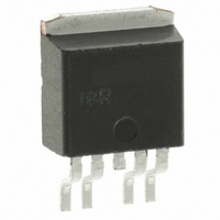
IR3312S International Rectifier, IR3312S Datasheet - Page 3

IR3312S
Manufacturer Part Number
IR3312S
Description
IC SWITCH HI-SIDE 50V 2.8A D2PAK
Manufacturer
International Rectifier
Type
High Sider
Datasheet
1.IR3312.pdf
(13 pages)
Specifications of IR3312S
Input Type
Non-Inverting
Number Of Outputs
1
On-state Resistance
15 mOhm
Current - Output / Channel
14A
Current - Peak Output
100A
Voltage - Supply
6 V ~ 28 V
Operating Temperature
-40°C ~ 150°C
Mounting Type
Surface Mount
Package / Case
D²Pak, TO-263 (4 leads + tab)
Lead Free Status / RoHS Status
Contains lead / RoHS non-compliant
Other names
*IR3312S
Static Electrical Characteristics
(T j = 25
4) Input thresholds are measured directly between the input pin and the tab. Any parasitic resistance in common between the load
5) Rds(on) is measured between the Tab and the Out pin, 5mm away from the package.
WWW.IRF.COM
Protection Characteristics
Tj = 25
Switching Electrical Characteristics
V cc = 14V, Resistive Load = 0.4 , T
Symbol
VIfb -Vin
Tsd
Treset
OV
Isdf
Isd_1k
Min.Pulse
WAIT
Rev.Rds on Rds(on) reverse battery protection
Symbol Parameter
Symbol
Iq
Iin
Vih
Vil
Vhys
Iout qs
Rds1 on
Rds2 on
Rds3 on
Vclamp1
Vclamp2
Vsd
Vaval.
Td on
T r1
T r2
E on
Td off
T f
E off
@ Isd
current path and the input signal path can significantly affect the thresholds.
o
o
C (unless otherwise specified), RIfb = 500 to 5kOhm.
C, V cc = 14V unless otherwise specified.)
Parameter
Over-current shutdown threshold
Over-temp. shutdown threshold
Protection reset time
Over voltage shutdown (not latched)
Fixed over current shutdown
Adjustable over current shutdown 1K
Minimum pulse width (no WAIT state)
WAIT function timer
Parameter
Total quiescent current (Iout +Ifb)
Input current
High level input threshold voltage (4)
Low level input threshold voltage (4)
Input hysterisis = Vih-Vil
Output quiescent current
ON state resistance (5)
ON state resistance (5)
ON state resistance (5)
Vcc to Vout active clamp voltage
Vcc to Vout active clamp voltage
Body diode forward voltage
Vcc to Vout avalanche voltage
Turn-on delay time to Vcc-Vout= 0.9 Vcc
Rise time to Vcc-Vout=5V
Rise time to V cc -V out = 0.1V cc
Turn ON energy
Turn-off delay to V cc -V out = 0.1V cc
Fall time to Vcc-Vout = 0.9 V cc
Turn OFF energy
j
= 25
o
C, (unless otherwise specified).
Min.
Min.
Min.
200
0.5
1.5
3.5
0.4
0.2
33
30
10
—
—
10
10
20
33
40
—
—
—
—
—
—
—
4
9
2
5
5
2
Typ.
Typ. Max. Units Test Conditions
Typ.
28.5
0.85
0.75
500
4.5
1.2
0.5
165
50
36
37
12
16
22
15
16
35
36
43
15
14
4
5
4
9
9
1
7
1
Max. Units Test Conditions
Max. Units Test Conditions
1200
300
5.4
3.5
5.5
1.5
1.5
41
45
16
28
50
50
—
15
20
28
38
—
40
20
60
60
25
—
6
1
1
5
m
ms
mA
m
°C
mJ
mJ
s
V
V
A
A
V
s
V
S
A
A
s
Vcc-Vin=0; Vcc-VIfb=0;
I out =15A, Tj = 150
Iout = 10mA
Vcc-Vin=0, Vcc-
Vcc-Vin=14V
Iout=15A, Vcc-Vin=14V
I out =10A, Vcc -Vin=6 V
Iout=5A
Iout=30A, Vcc-VIfb<20V
Iout=100mA,Vcc-Vfb> 35V
see Fig. 7
see Fig. 7
VIfb<Vin
RIfb=1k
see Fig. 6
see Figs. 6 and 7
Vcc-Vin=-12V, Iload=5A
see figure 2
see figure 3
IR3312(S)
Vcc-VIfb=12V
Vcc-Vout=12V
Vout=12V
o
C
3


