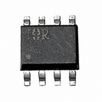
IPS022GTR International Rectifier, IPS022GTR Datasheet

IPS022GTR
Specifications of IPS022GTR
Available stocks
Related parts for IPS022GTR
IPS022GTR Summary of contents
Page 1
DUAL FULLY PROTECTED POWER MOSFET SWITCH Features Over temperature shutdown Over current shutdown Active clamp Low current & logic level input E.S.D protection Description The IPS022G are fully protected dual low side SMART POWER MOSFETs respectively. They feature over- current, ...
Page 2
IPS022G Absolute Maximum Ratings Absolute maximum ratings indicate sustained limits beyond which damage to the device may occur. All voltage parameters are referenced to SOURCE lead. (T Ambient = 25 print with 70 m copper thickness. Symbol Parameter V ds ...
Page 3
Recommended Operating Conditions These values are given for a quick design. For operation outside these conditions, please consult the application notes. Symbol Parameter V ds (max) Continuous drain to source voltage V IH High level input voltage V IL Low ...
Page 4
IPS022G Protection Characteristics Symbol Parameter T sd Over temperature threshold I sd Over current threshold V IN protection reset threshold reset T reset Time to reset protection EOI_OT Short circuit energy (see application note) Functional Block Diagram All values are ...
Page 5
Vin Ids t < T reset I shutdown Isd T T shutdown Tsd (165 °c) Figure 1 - Timing diagram Vin Ids Vds clamp ( Vcc ) Vds ( see Appl . Notes to evaluate power ...
Page 6
IPS022G All curves are typical values with standard footprints. Operating in the shaded area is not recommended. 300 250 200 150 100 Figure 5 - Rds Input Voltage ...
Page 7
Figure 9 - Turn-ON Delay Time, Rise Time & Time to 130% final Rds(on) (us Resistor ( ) 8 6 ...
Page 8
IPS022G 5 Std. footprint 127°C osfet on Std. footprint 100°C osfets - 100 Figure 13 - Max.Cont. Ids ( Amb. Temperature ( C) single pulse 10 ...
Page 9
Iin, Iin,off 0 -50 - 100 125 150 Figure 17 - Input Current (uA Junction Temperature ( C) 120% 115% 110% 105% 100% 95% ...
Page 10
IPS022G Case Outline 0.25 [.010 0.25 [.010 NOTES: 1. DIMENSIONING & T OLERANCING PER ASME Y14.5M-1994. ...


