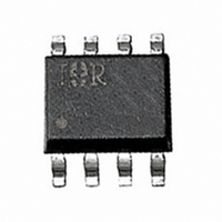
IPS022G International Rectifier, IPS022G Datasheet - Page 3

IPS022G
Manufacturer Part Number
IPS022G
Description
IC MOSFET LS DRIVER DUAL 8-SOIC
Manufacturer
International Rectifier
Type
Low Sider
Datasheet
1.IPS022G.pdf
(10 pages)
Specifications of IPS022G
Input Type
Non-Inverting
Number Of Outputs
2
On-state Resistance
130 mOhm
Current - Output / Channel
1A
Current - Peak Output
10A
Voltage - Supply
4 V ~ 6 V
Operating Temperature
-40°C ~ 150°C
Mounting Type
Surface Mount
Package / Case
8-SOIC (3.9mm Width)
Lead Free Status / RoHS Status
Contains lead / RoHS non-compliant
Other names
*IPS022G
Available stocks
Company
Part Number
Manufacturer
Quantity
Price
Company:
Part Number:
IPS022G
Manufacturer:
NXP
Quantity:
72 000
Part Number:
IPS022G
Manufacturer:
IR
Quantity:
20 000
Part Number:
IPS022GTRBPF
Manufacturer:
IR
Quantity:
20 000
Recommended Operating Conditions
These values are given for a quick design. For operation outside these conditions, please consult the application notes.
Static Electrical Characteristics
Standard footprint 70 m copper thickness. (T j = 25
www.irf.com
T r-in (max) Max recommended rise time for IN signal (see fig. 2)
R ds(on)
Switching Electrical Characteristics
V cc = 14V, Resistive Load = 10 , Rinput = 50
Symbol Parameter
T off
(2) Operations at higher switching frequencies is possible. See Appl. notes.
Symbol Parameter
V ds (max) Continuous drain to source voltage
V IH
V IL
I ds
R in
F r -I sc
Symbol Parameter
I dss 2
V
V
V in
V th
I in , -on
I in, -off
I dss 1
T on
T r
T rf
T f
Q in
clamp 1
clamp 2
clamp
(2)
( TAmbient = 85
High level input voltage
Low level input voltage
Continuous drain current
Recommended resistor in series with IN pin
Max. frequency in short circuit condition (Vcc = 14V)
ON state resistance T j = 25
Drain to source leakage current
Drain to source leakage current
Drain to source clamp voltage 1
Drain to source clamp voltage 2
IN to source clamp voltage
IN threshold voltage
ON state IN positive current
OFF state IN positive current
Turn-on delay time
Rise time
Time to 130% final R ds(on)
Turn-off delay time
Fall time
Total gate charge
o
C, IN = 5V, rth = 100
T j = 150
o
o
C
C
o
C/W, Tj = 85
100
o
C unless otherwise specified.)
s
pulse, T
Min.
Min.
0.15
100
0.4
0.8
0.5
48
50
25
50
o
—
—
0
0
7
1
2
C)
j
= 25
Typ.
Typ. Max. Units Test Conditions
0.01
130
220
130
0.1
1.5
0.5
0.9
1.3
3.3
54
56
90
8
6
2
o
C, (unless otherwise specified).
Max. Units Test Conditions
150
280
200
250
9.5
3.5
2.5
25
50
56
60
12
—
2
1
2
m
nC
V
A
A
s
Min.
—
4
0
—
0.5
—
0
V cc = 14V, T j = 25
V cc = 40V, T j = 25
I d = 20mA
I d =I shutdown
I in = 1 mA
I d = 50mA, V ds = 14V
V in = 5V
V in = 5V
over-current triggered
V in = 5V, I ds = 1A
See figure 2
V in = 5V
See figure 2
Max.
0.5
1
35
5
1
1
6
IPS022G
(see Fig.3 & 4)
(see Fig.3 & 4)
Units
kHz
k
o
o
A
V
S
C
C
3


