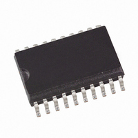
T6817-TKS Atmel, T6817-TKS Datasheet - Page 10

T6817-TKS
Manufacturer Part Number
T6817-TKS
Description
IC DRIVER DUAL TRPL DMOS 20-SSOP
Manufacturer
Atmel
Type
High Side/Low Side Driverr
Datasheet
1.T6817-TKQ.pdf
(16 pages)
Specifications of T6817-TKS
Input Type
Serial
Number Of Outputs
6
On-state Resistance
2 Ohm, 1.5 Ohm
Current - Output / Channel
600mA
Current - Peak Output
950mA
Voltage - Supply
7 V ~ 40 V
Operating Temperature
-40°C ~ 150°C
Mounting Type
Surface Mount
Package / Case
20-SOIC (5.3mm Width), 20-SO, 20-SOEIAJ
For Use With
ATAB6817 - BOARD EVAL FOR T6817
Lead Free Status / RoHS Status
Contains lead / RoHS non-compliant
8. Electrical Characteristics (Continued)
7.5V < V
10
*) Type means: A =100% tested, B = 100% correlation tested, C = Characterized on samples, D = Design parameter
Note:
5.13
5.14
5.15
5.16
5.17
5.18
No.
6.1
6.2
6.3
6.4
7.1
7.2
7.3
7.4
7.5
8.1
8.2
8.3
6
7
8
VS
Parameters
Open load detection
current
Open load detection
current ratio
Open load detection
threshold
Open load detection
threshold
Output switch on
delay
Output switch off
delay
Inhibit Input
Input voltage low
level threshold
Input voltage high
level threshold
Hysteresis of input
voltage
Pull-down current
Serial Interface – Logic Inputs DI, CLK, CS
Input voltage
low-level threshold
Input voltage
high-level threshold
Hysteresis of input
voltage
Pull-down current pin
DI, CLK
Pull-up current
pin CS
Serial Interface - Logic Output DO
Output voltage low
level
Output voltage high
level
Leakage current
(tri-state)
1. Delay time between rising edge of CS after data transmission and switch on/off output stages to 90% of final level
T6817
< V
OV
(1)
(1)
; 4.5V < V
VCC
< 5.5V; INH = High; –40°C < T
Test Conditions
Input register bit 13
(OLD) = low, output off
Input register bit 13
(OLD) = low, output off
Input register bit 13
(OLD) = low, output off
R
R
V
V
V
I
I
V
0 V < V
OL
OL
INH
DI
CS
CS
Load
Load
, V
= 3 mA
= –2 mA
= 0V
= V
= V
= 1 k
= 1 k
CLK
VCC,
DO
VCC
= V
< V
VCC
VCC
12, 14,
12, 14,
j
8, 15,
< 150°C; unless otherwise specified, all values refer to GND pins.
2, 4
Pin
2-4
2-4
2-4
16
17
16
18
18
18
5
5
5
5
3
Symbol
V
V
I
I
I
V
V
V
HS1–3
LS1–3/
HS1–3
I
I
HS1–3
t
t
LS1–3
V
V
PDSI
PUSI
I
V
I
V
don
doff
DOL
DOH
DO
VS–
PD
V
V
IH
IH
IL
IL
I
I
0.3
0.3
–150
V
V
V
Min.
100
–50
–1V
–10
1.2
0.6
0.6
10
50
VCC
VCC
VCC
2
Typ.
0.7
0.7
Max.
V
V
–30
700
500
0.5
0.5
80
50
–2
10
VCC
VCC
2
2
1
Unit
mV
mV
ms
ms
µA
µA
µA
µA
µA
V
V
V
V
V
V
V
V
4670E–BCD–04/09
Type*
A
A
A
A
A
A
A
A
A
A
A
A
A
A
A
A
A
A


