IPS7081RPBF International Rectifier, IPS7081RPBF Datasheet
IPS7081RPBF
Specifications of IPS7081RPBF
Available stocks


Related parts for IPS7081RPBF

IPS7081RPBF Summary of contents
Page 1
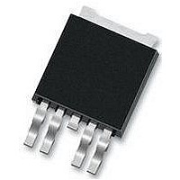
... Product Summary Package IPS7081PbF IPS7081SPbF +5V +Bat 15K Dg(4) Control In(2) Gnd(1) Rin Data sheet N° PD60308 IPS7081(R)(S)PbF Rds(on) 70m Vclamp 70V I Limit 5A (typ.) Open load 3V TO220 D²Pak IPS7081RPbF Vcc(3) Pull-up resistor for Open Load Off detection Out(5) Load Ω max. D-Pak 1 ...
Page 2
Absolute Maximum Ratings Absolute maximum ratings indicate sustained limits beyond which damage to the device may occur. All voltage parameters are referenced to Ground lead. (Tambient=25°C unless otherwise specified). Symbol Parameter Vout Maximum output voltage Voffset Maximum logic ground to ...
Page 3
Static Electrical Characteristics Tj=25°C, Vcc=14V (unless otherwise specified) Symbol Parameter ON state resistance Tj=25°C Rds(on) ON state resistance Tj=150°C ON state resistance Tj=25°C, Vcc=6.5V Vcc op. Operating voltage range V clamp 1 Vcc to Out clamp voltage 1 V clamp ...
Page 4
Protection Characteristics Symbol Parameter Ilim Internal current limit Tsd+ Over temperature high threshold Tsd- Over temperature low threshold Vsc Short-circuit detection voltage Vopen load Open load detection threshold (1 ) Guarantee design (2 ) Reference to Vcc ...
Page 5
Functional Block Diagram All values are typical 75V IN 6V Gnd DG 6V GND www.irf.com 165°C Tj 158°C Vcc-Gnd >UV Level 2.5V Sh ifter 2.0V Loss Protection Open Load Short Circuit IPS7081(R)(S) VCC 66V Charge Pump Driver - + I ...
Page 6
Vin Ids Vds clamp Vds Vcc See Application Notes to evaluate power dissipation Figure 1 – Active clamp waveforms 90% Vin Vih 10% 90% Vcc-5V Vout 10 Tr1 Vds Figure 3 – Switching times definition www.irf.com T clamp ...
Page 7
Dg In Gnd 5V Vin 0V Rem : During active clamp, Vload is negative Figure 5 – Active clamp test circuit -50 0 Tamb, Ambient temperature (°C) Figure 7 – Max. ouput current (A) ...
Page 8
Tj, junction temperature (°C) Figure 9 –I limit (A) Vs junction temperature (°C) 200% 150% 100% 50% -50 0 Tj, junction temperature (°C) Figur Normalized Rds(on) (%) Vs T ...
Page 9
Vcc, power supply voltage (V) Figure 13 – Icc on/ Icc off (µA) V www.irf.com Icc on Icc off Vcc (V) IPS7081(R)(S) 1.E+4 1.E+3 1.E+2 1.E+1 ...
Page 10
Case outline – TO220 – 5 leads www.irf.com IPS7081(R)(S) 10 ...
Page 11
Case Outline – D²pak – 5 leads www.irf.com IPS7081(R)(S) 11 ...
Page 12
Tape and Reel – D²Pak – 5 leads www.irf.com IPS7081(R)(S) 12 ...
Page 13
Case Outline – Dpak – 5 leads www.irf.com IPS7081(R)(S) 13 ...
Page 14
Tape & Reel – Dpak – 5 leads IR WORLD HEADQUARTERS: This product has been designed and qualified for the Automotive [Q100] market. www.irf.com 233 Kansas St., El Segundo, California 90245 Tel: (310) 252-7105 Data and specifications subject to change ...