MAX4821EUP+ Maxim Integrated Products, MAX4821EUP+ Datasheet - Page 6
MAX4821EUP+
Manufacturer Part Number
MAX4821EUP+
Description
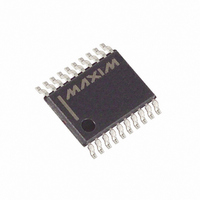
IC RELAY DRIVER 8CHAN 20-TSSOP
Manufacturer
Maxim Integrated Products
Type
Relay/Lamp Driverr
Datasheet
1.MAX4821EUP.pdf
(12 pages)
Specifications of MAX4821EUP+
Input Type
Parallel/Serial
Number Of Outputs
8
On-state Resistance
2 Ohm
Current - Output / Channel
70mA
Current - Peak Output
150mA
Voltage - Supply
2.3 V ~ 5.5 V
Operating Temperature
-40°C ~ 85°C
Mounting Type
Surface Mount
Package / Case
20-TSSOP
Product
Relay Drivers
Rise Time
2 us
Fall Time
2 us
Supply Voltage (max)
5.5 V
Supply Voltage (min)
2.3 V
Supply Current
50 uA
Maximum Power Dissipation
1739 mW
Maximum Operating Temperature
+ 85 C
Mounting Style
SMD/SMT
Maximum Turn-off Delay Time
1 us
Maximum Turn-on Delay Time
1 us
Minimum Operating Temperature
- 40 C
Number Of Drivers
8
Output Current
70 mA
Output Voltage
0.4 V
Device Type
Relay
Supply Voltage Range
2.3V To 5.5V
Driver Case Style
TSSOP
No. Of Pins
20
Operating Temperature Range
-40°C To +85°C
Filter Terminals
SMD
Rohs Compliant
Yes
Lead Free Status / RoHS Status
Lead free / RoHS Compliant


+3.3V/+5V, 8-Channel, Cascadable Relay Drivers
with Serial/Parallel Interface
The MAX4820/MAX4821 8-channel relay drivers offer
built-in kickback protection and drive +3.3V/+5V non-
latching or dual-coil-latching relays. These devices are
especially useful when driving +3V relays. Each inde-
pendent open-drain output features a 2Ω on-resistance
and is guaranteed to sink 70mA (min) load current. Both
devices consume less than 50µA (max) quiescent cur-
rent and feature 1µA (min) output off-leakage current.
The MAX4820 features an SPI/QSPI/MICROWIRE-com-
patible serial interface. Input data is shifted into an 8-bit
shift register and latched to the outputs when CS transi-
tions from low to high. Each data bit in the shift register
corresponds to a specific output, allowing independent
control of all outputs.
6
THIN
QFN
12
13
14
15
17
18
19
20
—
—
—
—
—
_______________________________________________________________________________________
MAX4820
TSSOP
14
15
16
17
19
20
—
—
—
—
—
1
2
PIN
THIN
QFN
12
13
14
15
17
18
19
20
Detailed Description
—
3
4
5
6
MAX4821
TSSOP
14
15
16
17
19
20
—
1
2
5
6
7
8
NAME
OUT5
OUT4
OUT3
OUT2
OUT1
COM
V
SET
LVL
A0
A1
A2
EP
CC
Open-Drain Output 5. Connect OUT5 to the low side of a relay coil. This
output is pulled to PGND when activated, but otherwise is high impedance.
Common Free-Wheeling Diodes. Connect COM to V
connected to a separate supply that is higher than V
V
Open-Drain Output 4. Connect OUT4 to the low side of a relay coil. This
output is pulled to PGND when activated, but otherwise is high impedance.
Open-Drain Output 3. Connect OUT3 to the low side of a relay coil. This
output is pulled to PGND when activated, but otherwise is high impedance.
Open-Drain Output 2. Connect OUT2 to the low side of a relay coil. This
output is pulled to PGND when activated, but otherwise is high impedance.
Open-Drain Output 1. Connect OUT1 to the low side of a relay coil. This
output is pulled to PGND when activated, but otherwise is high impedance.
Input Supply Voltage. Bypass V
Set Input. Drive SET low to set all latches and registers high (all outputs are
turned on). SET overrides all parallel and serial control inputs. RESET
overrides SET under all conditions.
Level Input. LVL determines whether the selected address is switched on or
off. A logic high on LVL switches on the addressed output. A logic low on
LVL switches off the addressed output.
Digital Address “0” Input. (See Table 2 for address mapping.)
Digital Address “1” Input. (See Table 2 for address mapping.)
Digital Address “2” Input. (See Table 2 for address mapping.)
Exposed Pad. Connect exposed pad to GND.
CC
to GND with a 0.1µF capacitor.
The MAX4821 features a 4-bit (A0, A1, A2, LVL) parallel
input interface. The three bits (A0, A1, A2) determine
the output address, and LVL determines whether the
selected output is switched on or off. Data is latched to
the outputs when CS transitions from low to high.
Both devices feature separate set and reset functions
that allow the user to turn on or turn off all outputs
simultaneously with a single control line. Built-in hys-
teresis (Schmidt trigger) on all digital inputs allows this
device to be used with slow rising and falling signals,
such as those from optocouplers or RC power-up ini-
tialization circuits. The MAX4820/MAX4821 are avail-
able in 20-pin TSSOP and space-saving 20-pin Thin
QFN packages.
Pin Description (continued)
CC
FUNCTION
to GND with a 0.1µF capacitor.
CC
CC
. COM can also be
. In that case, bypass
Related parts for MAX4821EUP+
Image
Part Number
Description
Manufacturer
Datasheet
Request
R

Part Number:
Description:
MAX7528KCWPMaxim Integrated Products [CMOS Dual 8-Bit Buffered Multiplying DACs]
Manufacturer:
Maxim Integrated Products
Datasheet:
Part Number:
Description:
Single +5V, fully integrated, 1.25Gbps laser diode driver.
Manufacturer:
Maxim Integrated Products
Datasheet:
Part Number:
Description:
Single +5V, fully integrated, 155Mbps laser diode driver.
Manufacturer:
Maxim Integrated Products
Datasheet:
Part Number:
Description:
VRD11/VRD10, K8 Rev F 2/3/4-Phase PWM Controllers with Integrated Dual MOSFET Drivers
Manufacturer:
Maxim Integrated Products
Datasheet:
Part Number:
Description:
Highly Integrated Level 2 SMBus Battery Chargers
Manufacturer:
Maxim Integrated Products
Datasheet:
Part Number:
Description:
Current Monitor and Accumulator with Integrated Sense Resistor; ; Temperature Range: -40°C to +85°C
Manufacturer:
Maxim Integrated Products
Part Number:
Description:
TSSOP 14/A�/RS-485 Transceivers with Integrated 100O/120O Termination Resis
Manufacturer:
Maxim Integrated Products
Part Number:
Description:
TSSOP 14/A�/RS-485 Transceivers with Integrated 100O/120O Termination Resis
Manufacturer:
Maxim Integrated Products
Part Number:
Description:
QFN 16/A�/AC-DC and DC-DC Peak-Current-Mode Converters with Integrated Step
Manufacturer:
Maxim Integrated Products
Part Number:
Description:
TDFN/A/65V, 1A, 600KHZ, SYNCHRONOUS STEP-DOWN REGULATOR WITH INTEGRATED SWI
Manufacturer:
Maxim Integrated Products
Part Number:
Description:
Integrated Temperature Controller f
Manufacturer:
Maxim Integrated Products
Part Number:
Description:
SOT23-6/I�/45MHz to 650MHz, Integrated IF VCOs with Differential Output
Manufacturer:
Maxim Integrated Products
Part Number:
Description:
SOT23-6/I�/45MHz to 650MHz, Integrated IF VCOs with Differential Output
Manufacturer:
Maxim Integrated Products
Part Number:
Description:
EVALUATION KIT/2.4GHZ TO 2.5GHZ 802.11G/B RF TRANSCEIVER WITH INTEGRATED PA
Manufacturer:
Maxim Integrated Products
Part Number:
Description:
QFN/E/DUAL PCIE/SATA HIGH SPEED SWITCH WITH INTEGRATED BIAS RESISTOR
Manufacturer:
Maxim Integrated Products
Datasheet: