NIF5003NT1G ON Semiconductor, NIF5003NT1G Datasheet
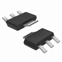
MOSFET N-CH HD+ 14A 42V SOT223

NIF5003NT1G

Manufacturer Part Number
NIF5003NT1G
Description
MOSFET N-CH HD+ 14A 42V SOT223
Manufacturer
ON Semiconductor
Series
HDPlus™r
Type
Low Sider
Datasheet

Specifications of NIF5003NT1G

Input Type
Non-Inverting
Number Of Outputs
1
On-state Resistance
53 mOhm
Current - Peak Output
14A
Operating Temperature
-55°C ~ 150°C
Mounting Type
Surface Mount
Package / Case
SOT-223 (3 leads + Tab), SC-73, TO-261
Configuration
Single Dual Drain
Transistor Polarity
N-Channel
Resistance Drain-source Rds (on)
0.053 Ohm (Typ) @ 10 V
Drain-source Breakdown Voltage
42 V
Gate-source Breakdown Voltage
+/- 14 V
Continuous Drain Current
14 A
Power Dissipation
1900 mW
Maximum Operating Temperature
+ 150 C
Mounting Style
SMD/SMT
Minimum Operating Temperature
- 55 C
Continuous Drain Current Id
14A
Drain Source Voltage Vds
42V
On Resistance Rds(on)
53mohm
Rds(on) Test Voltage Vgs
10V
Threshold Voltage Vgs Typ
1.7V
Rohs Compliant
Yes
Lead Free Status / RoHS Status
Lead free / RoHS Compliant
Voltage - Supply
-
Current - Output / Channel
-
Lead Free Status / Rohs Status
Lead free / RoHS Compliant
Other names
NIF5003NT1GOS
NIF5003NT1GOS
NIF5003NT1GOSTR

Available stocks

Company
Part Number
Manufacturer
Quantity
Price
Part Number:
NIF5003NT1G
Manufacturer:
ON
Quantity:
996
Part Number:
NIF5003NT1G
Manufacturer:
ON/安森美
Quantity:
20 000
NIF5003N
Self-Protected FET
with Temperature and
Current Limit
42 V, 14 A, Single N−Channel, SOT−223
utilize ON Semiconductors latest MOSFET technology process to
achieve the lowest possible on−resistance per silicon area while
incorporating smart features. Integrated thermal and current limits
work together to provide short circuit protection. The devices feature
an integrated Drain−to−Gate Clamp that enables them to withstand
high energy in the avalanche mode. The Clamp also provides
additional safety margin against unexpected voltage transients.
Electrostatic Discharge (ESD) protection is provided by an integrated
Gate−to−Source Clamp.
Features
Stresses exceeding Maximum Ratings may damage the device. Maximum Ratings
are stress ratings only. Functional operation above the Recommended Operating
Conditions is not implied. Extended exposure to stresses above the Recommended
Operating Conditions may affect device reliability.
1. Surface mounted onto minimum pad size (0.412″ square) FR4 PCB, 1 oz cu.
2. Mounted onto 1″ square pad size (1.127″ square) FR4 PCB, 1 oz cu.
3. Normal pre−fault operating range. See thermal limit range conditions.
MAXIMUM RATINGS
© Semiconductor Components Industries, LLC, 2008
September, 2008 − Rev. 5
Drain−to−Source Voltage Internally Clamped
Gate−to−Source Voltage
Drain Current
Total Power Dissipation
Thermal Resistance
Single Pulse Drain−to−Source Avalanche Energy
Operating and Storage Temperature Range
(Note 3)
HDPlus™ devices are an advanced series of power MOSFETs which
Short Circuit Protection/Current Limit
Thermal Shutdown with Automatic Restart
I
Avalanche Energy Specified
Slew Rate Control for Low Noise Switching
Overvoltage Clamped Protection
Pb−Free Packages are Available
DSS
@ T
@ T
Junction−to−Case
Junction−to−Ambient (Note 1)
Junction−to−Ambient (Note 2)
(V
I
L
DD
= 7.0 Apk, L = 9.5 mH, R
Specified at Elevated Temperature
A
A
= 25 Vdc, V
= 25°C (Note 1)
= 25°C (Note 2)
Rating
Continuous
GS
(T
= 5.0 Vdc,
J
= 25°C unless otherwise noted)
Preferred Device
G
= 25 W)
Symbol
T
V
R
R
R
J
V
E
P
DSS
, T
I
qJC
qJA
qJA
GS
AS
D
D
stg
−55 to 150
Internally Limited
Value
"14
1.25
100
233
1.9
42
12
65
1
°C/W
Unit
Vdc
Vdc
mJ
°C
W
See detailed ordering and shipping information in the package
dimensions section on page 4 of this data sheet.
Preferred devices are recommended choices for future use
and best overall value.
Gate
Input
(Clamped)
V
42 V
(Note: Microdot may be in either location)
DSS
ESD Protection
SOURCE
A
Y
W
5003N = Specific Device Code
G
ORDERING INFORMATION
1
DRAIN
Temperature
GATE
R
MARKING DIAGRAM
2
G
http://onsemi.com
http://onsemi.com
Limit
3
53 mW @ 10 V
= Assembly Location
= Year
= Work Week
= Pb−Free Package
R
Overvoltage
4
1
2
3
Protection
DS(on)
Publication Order Number:
CASE 318E
TYP
SOT−223
Current
STYLE 3
Limit
4
DRAIN
Drain
(Limited)
Current
NIF5003N/D
Sense
I
Source
D
14 A
MAX
M
PWR

Related parts for NIF5003NT1G

NIF5003NT1G Summary of contents

Page 1

... Current Limit Single N−Channel, SOT−223 HDPlus™ devices are an advanced series of power MOSFETs which utilize ON Semiconductors latest MOSFET technology process to achieve the lowest possible on−resistance per silicon area while incorporating smart features. Integrated thermal and current limits work together to provide short circuit protection. The devices feature an integrated Drain− ...

Page 2

MOSFET ELECTRICAL CHARACTERISTICS Characteristic OFF CHARACTERISTICS Drain−to−Source Clamped Breakdown Voltage ( Vdc 250 mAdc Vdc 250 mAdc −40°C to 150° Zero Gate Voltage Drain ...

Page 3

Current Limit Inception Region 25° 0.5 1 1 ...

Page 4

... ORDERING INFORMATION Device NIF5003NT1 NIF5003NT1G NIF5003NT3 NIF5003NT3G †For information on tape and reel specifications, including part orientation and tape sizes, please refer to our Tape and Reel Packaging Specifications Brochure, BRD8011/D. TYPICAL PERFORMANCE CURVES 25°C J 0.5 0.6 0.7 0 SOURCE−TO−DRAIN VOLTAGE (VOLTS) SD Figure 7 ...

Page 5

... A1 *For additional information on our Pb−Free strategy and soldering details, please download the ON Semiconductor Soldering and Mounting Techniques Reference Manual, SOLDERRM/D. HDPlus is a trademark of Semiconductor Components Industries, LLC (SCILLC) ON Semiconductor and are registered trademarks of Semiconductor Components Industries, LLC (SCILLC). SCILLC reserves the right to make changes without further notice to any products herein ...

Related keywords