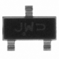
MDC3105LT1G ON Semiconductor, MDC3105LT1G Datasheet - Page 9

MDC3105LT1G
Manufacturer Part Number
MDC3105LT1G
Description
IC RELAY/DRVR INDUCT LOAD SOT23
Manufacturer
ON Semiconductor
Type
Relay/Load Driverr
Specifications of MDC3105LT1G
Input Type
Non-Inverting
Number Of Outputs
1
Current - Output / Channel
400mA
Current - Peak Output
500mA
Voltage - Supply
6V
Operating Temperature
-40°C ~ 85°C
Mounting Type
Surface Mount
Package / Case
SOT-23-3, TO-236-3, Micro3™, SSD3, SST3
Supply Voltage Max
6V
No. Of Outputs
1
Output Current
400mA
Driver Case Style
SOT-23
Device Type
Relay
Filter Terminals
SMD
No. Of Pins
3
Rohs Compliant
Yes
Leaded Process Compatible
Yes
Lead Free Status / RoHS Status
Lead free / RoHS Compliant
On-state Resistance
-
Lead Free Status / Rohs Status
Lead free / RoHS Compliant
Other names
MDC3105LT1GOS
MDC3105LT1GOS
MDC3105LT1GOSTR
MDC3105LT1GOS
MDC3105LT1GOSTR
Available stocks
Company
Part Number
Manufacturer
Quantity
Price
Company:
Part Number:
MDC3105LT1G
Manufacturer:
ON Semiconductor
Quantity:
127 439
Company:
Part Number:
MDC3105LT1G
Manufacturer:
ON Semiconductor
Quantity:
2 500
Part Number:
MDC3105LT1G
Manufacturer:
ON/安森美
Quantity:
20 000
1.
2.
3.
4.
5.
Determine the maximum inductive load current (at
max V
temperature) that the MDC3105 will have to drive
and make sure it is less than the max rated current.
For pulsed operation, use the Transient Thermal
Response of Figure 12 and the instructions with it
to determine the maximum limit on transistor power
dissipation for the desired duty cycle and
temperature range.
Use Figures 10 and 11 with the SOA notes above to
insure that instantaneous operation does not push
the device beyond the limits of the SOA plot.
While keeping any V
determine the max input current needed to achieve
that output current from Figures 2 and 6.
For levels of input current below 100 mA, use the
input threshold curves of Figure 4 to verify that
EQUIVALENT
74HC04 OR
Designing with this Data Sheet
CC
+3.0 ≤ V
, min coil resistance and usually minimum
DD
≤ +3.75 Vdc
O(sat)
Figure 13. A 200 mW, 5.0 V Dual Coil Latching Relay Application
V
in
(5)
requirements in mind,
with 3.0 V−HCMOS Level Translating Interface
+4.5 ≤ V
GND (1)
APPLICATIONS DIAGRAMS
V
out
(6)
http://onsemi.com
CC
≤ +5.5 Vdc
MDC3105DMT1
TX2-L2-5 V
AROMAT
+
9
+
6.
7.
8.
9.
there will be adequate input current available to
turn on the MDC3105 at all temperatures.
For levels of input current above 100 mA, enter
Figure 3 using that max input current and determine
the input voltage required to drive the MDC3105
from the solid V
drive source family from those whose dotted lines
cross the solid input characteristic line to the right
of the I
Using the max output current calculated in step 1,
check Figure 7 to insure that the range of Zener
clamp voltage over temperature will satisfy all
system and EMI requirements.
Using Figures 8 and 9, insure that “OFF” state
leakage over temperature and voltage extremes does
not violate any system requirements.
Review circuit operation and insure none of the
device max ratings are being exceeded.
GND (4)
V
out
(3)
in
, V
in
point.
in
versus I
V
in
(2)
in
line. Select a suitable
EQUIVALENT
74HC04 OR


