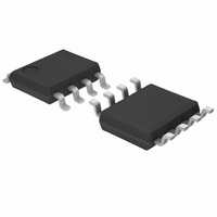
BD2056AFJ-E2 Rohm Semiconductor, BD2056AFJ-E2 Datasheet - Page 6

BD2056AFJ-E2
Manufacturer Part Number
BD2056AFJ-E2
Description
IC SWITCH HIGH SIDE 2CH SOP-J8
Manufacturer
Rohm Semiconductor
Type
High Sider
Specifications of BD2056AFJ-E2
Input Type
Non-Inverting
Number Of Outputs
2
On-state Resistance
100 mOhm
Current - Output / Channel
250mA
Current - Peak Output
500mA
Voltage - Supply
2.7 V ~ 5.5 V
Operating Temperature
-40°C ~ 85°C
Mounting Type
Surface Mount
Package / Case
8-SOPJ
Primary Input Voltage
5V
No. Of Outputs
1
Output Voltage
5V
Output Current
250mA
Voltage Regulator Case Style
SOP
No. Of Pins
8
Operating Temperature Range
-40°C To +85°C
Svhc
No SVHC
Output Power
560 mW
Input Voltage
2.7 V to 5.5 V
Mounting Style
SMD/SMT
Lead Free Status / RoHS Status
Lead free / RoHS Compliant
Lead Free Status / RoHS Status
Lead free / RoHS Compliant, Lead free / RoHS Compliant
Other names
BD2056AFJ-E2TR
Waveform data
© 2009 ROHM Co., Ltd. All rights reserved.
BD2046AFJ, BD2056AFJ
www.rohm.com
(0.5A/div.)
(5V/div.)
I
V
(5V/div.)
(0.5A/div.)
(5V/div.)
(0.5A/div.)
(5V/div.)
I
V
(5V/div.)
I
OUT
(0.5A/div.)
(5V/div.)
V
(5V/div.)
(5V/div.)
I
V
V
(5V/div.)
V
V
V
OUT
OUT
(5V/div.)
V
(5V/div.)
OUT
V
V
/EN
/OC
/OC
OUT
OUT
/OC
OUT
/OC
/EN
/OC
OUT
Regarding the output rise/fall and over current detection characteristics of BD2046AFJ, refer to the characteristic of BD2056AFJ.
Fig.26 Output rise characteristic
Fig.29 Over current response
Fig.31 Over current response
Fig.34 UVLO response
Enable to short circuit
Increasing V
(BD2056AFJ)
(BD2056AFJ)
Ramped load
(BD2056AFJ)
(BD2056AFJ)
TIME(20ms/div.)
TIME (2ms/div.)
TIME (1s/div.)
TIME(1ms/div.)
IN
C
V
R
C
V
IN
L
IN
L
L
V
=100uF
=10Ω
=100uF
R
C
=5V
=5V
IN
L
L
=5V
=20Ω
=100uF
(5V/div.)
(5V/div.)
V
V
(0.5A/div.)
(5V/div.)
(5V/div.)
I
V
(0.5A/div.)
V
(5V/div.)
(0.5A/div.)
OUT
V
I
I
(1V/div.)
/EN
/OC
OUT
(1V/div.)
V
OUT
/OC
OUT
V
OUT
(0.5A/div.)
I
OUT
(5V/div.)
(5V/div.)
(5V/div.)
/OC
V
V
OUT
V
/OC
OUT
/OC
Fig.27 Output fall characteristic
Fig.32 Over current response
Fig.30 Over current response
R
C
L
L
Enable to short circuit
=20Ω
=100uF
Fig.35 UVLO response
(BD2056AFJ)
(BD2056AFJ)
Decreasing V
Ramped load
(BD2056AFJ)
TIME (1ms/div.)
TIME(1ms/div.)
(BD2056AFJ)
TIME(2ms/div.)
6/13
TIME (1s/div.)
C
V
V
R
C
IN
L
IN
L
L
=100uF
V
=2.5V
=10Ω
=100uF
=5V
IN
IN
=5V
(0.1A/div.)
I
(0.5A/div.)
(1V/div.)
I
V
(1V/div.)
V
OUT
OUT
(5V/div.)
V
(5V/div.)
V
/EN
/OC
OUT
/OC
Fig.28 Inrush current response
Fig.33 Over current response
Enable to short circuit
(BD2056AFJ)
(BD2056AFJ)
CL=47µF
TIME (500ms/div.)
Thermal Shutdown
TIME(500us/div.)
CL=100µ
CL=200µF
Technical Note
2009.05 - Rev.A
CL=147µF
V
R
V
C
IN
L
=20Ω
IN
L
=5V
=100uF
=5V


