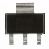
ZXMS6001N3TA Diodes Zetex, ZXMS6001N3TA Datasheet

ZXMS6001N3TA
Specifications of ZXMS6001N3TA
Available stocks
Related parts for ZXMS6001N3TA
ZXMS6001N3TA Summary of contents
Page 1
... Thermal shutdown with auto restart • Over-current protection • Input protection (ESD) • Load dump protection (actively protects load) • Low input current Ordering information Device Package ZXMS6001N3TA SOT223 Issue 1 - January 2008 © Zetex Semiconductors plc 2008 = 60V DS 675mΩ 1. 5V 5V) ...
Page 2
Functional block diagram IN Human body ESD protection Applications and information • Especially suited for loads with a high in-rush current such as lamps and motors. • All types of resistive, inductive and capacitive loads in switching applications. µC compatible ...
Page 3
Absolute maximum ratings Parameter Continuous Drain-Source Voltage Drain-Source Voltage for short circuit protection V Continuous Input Voltage Peak Input Voltage Continuous Input Current -0.2V=V =10V IN V <-0. >10V IN IN Operating Temperature Range Storage Temperature Range Power ...
Page 4
Recommended operating conditions The ZXMS6001 is optimized for use with µC operating from 5V supplies. Symbol Description V Input voltage range IN T Ambient temperature range A V High level input voltage for MOSFET IH V Peripheral supply voltage P ...
Page 5
Parameter Protection Functions (f) Minimum input voltage for over temperature protection Maximum input voltage for over temperature protection Thermal Overload Trip Temperature Thermal hysteresis Unclamped single pulse inductive energy Tj=25°C Unclamped single pulse inductive energy Tj=150°C Inverse Diode Source drain ...
Page 6
Application information The current-limit protection circuitry is designed to de-activate at low Vds to prevent the load current from being unnecessarily restricted during normal operation. The design max DC operating current is therefore determined by the thermal capability of the ...
Page 7
Large copper area characteristics For large copper area as described in note (a) Max Ambient Temperature T 25°C at Vin=5V 70°C at Vin=5V 85°C at Vin=5V 125°C at Vin=5V R DS(on) Limited 100m 100ms 10ms Single Pulse ...
Page 8
Current limit inactive Current limit active Drain-Source Voltage (V) DS Typical Output Characteristic 1.4 1.2 1.0 0.8 0.6 ...
Page 9
Package outline - SOT223 Millimeters Dim. Min. Max 1.80 A1 0.02 0.10 A2 1.55 1.65 b 0.66 0.84 b2 2.90 3.10 C 0.23 0.33 Note: Controlling dimensions are in millimeters. Approximate dimensions are provided in inches Issue 1 ...
Page 10
Definitions Product change Zetex Semiconductors reserves the right to alter, without notice, specifications, design, price or conditions of supply of any product or service. Customers are solely responsible for obtaining the latest relevant information before placing orders. Applications disclaimer The ...


