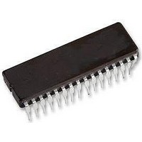
MC33395EW Freescale Semiconductor, MC33395EW Datasheet - Page 11

MC33395EW
Manufacturer Part Number
MC33395EW
Description
IC GATE DRIVER 3PHASE 32-SOICW
Manufacturer
Freescale Semiconductor
Type
3 Phase Brushless DC Motor Controllerr
Datasheet
1.MC33395TEWR2.pdf
(16 pages)
Specifications of MC33395EW
Configuration
3 Phase Bridge
Input Type
Non-Inverting
Delay Time
3µs
Number Of Configurations
1
Number Of Outputs
3
Voltage - Supply
5.5 V ~ 24 V
Operating Temperature
-40°C ~ 125°C
Mounting Type
Surface Mount
Package / Case
32-SOIC (7.5mm Width)
Operating Temperature Classification
Automotive
Package Type
SOIC W
Operating Supply Voltage (min)
-0.3V
Operating Supply Voltage (max)
7V
Operating Supply Voltage
- 0.3 V to + 7 V
Supply Current
1.8 mA
Mounting Style
SMD/SMT
Lead Free Status / RoHS Status
Lead free / RoHS Compliant
Current - Peak
-
High Side Voltage - Max (bootstrap)
-
Lead Free Status / Rohs Status
Compliant
Figure
required to turn ON and hold ON the low-side MOSFETs, as
well as turn OFF the MOSFETs.
V
will blow and set all outputs of the device to OFF, if the V
voltage exceeds that stated in the maximum rating section of
the data sheet. When this fuse blows, the device is
permanently disabled.
I
current sense comparator. In a typical application, these
would receive a a low-pass filtered voltage derived from a
current sense resistor placed in series with the ground return
of the three-phase output bridge. When triggered by the
comparator, the CL (current limit) bit of the internal error
register is set, and the output gate drive pairs (i.e., GDH1 and
GDL1, GDH2 and GDL2, GDH3 and GDL3), are controlled
such that current will cease flowing through the load (refer to
Table
OVERTEMPERATURE AND OVERVOLTAGE
SHUTDOWN CIRCUITS
conditions and over voltage conditions. When any of these
conditions presents itself to the IC, the corresponding
internally set bits of the error register are set, and the output
gate drive pairs (i.e., GDH1 and GDL1, GDH2 and GDL2,
GDH3 and GDL3), are controlled such that current will cease
flowing through the load (refer to
LSE AND HSE INPUT CIRCUITS
high-side enable input pins (HSE1, HSE2, HSE3) form the
input pairs (HSE1 and LSE1, HSE2 and LSE2, HSE3 and
LSE3) which set the logic states of the output gate drive pairs
(i.e., GDH1 and GDL1, GDH2 and GDL2, GDH3 and GDL3)
in accordance with the logic set forth in the Truth Table
(page
or DSP to provide the phasing of the currents applied to a
brushless dc motor's stator coils via the output MOSFET
pairs.
PWM INPUT
pin to accomplish PWM modulation of the output pairs in
accordance with the states of the Mode 0 and Mode 1 inputs
as set forth in the Truth Table
MODE SELECTION INPUTS
determine the PWM implementation of the output pairs in
accordance with the logic set forth in the Truth Table
(page
high-side MOSFETs or the low-side MOSFETs, or can be set
Analog Integrated Circuit Device Data
Freescale Semiconductor
SENS
DD
The V
The +I
Internal monitoring is provided for both over temperature
The low-side enable input pins (LSE1, LSE2, LSE3) and
The pulse width modulation input provides a single input
The mode selection inputs (Mode 0 and Mode 1)
FUSE
5, Truth Table, page 12).
12). Typically these inputs are supplied from an MCU
12). PWMing can thus be set to occur either on the
INPUTS
5). These gate drive outputs supply the peak currents
DD
sens
supply of the 33395 IC has an internal fuse, which
and -I
sens
pins are inputs to the internal
(page
Table
12).
5).
DD
to occur on both the high-side and low-side MOSFETs as
"complementary chopping".
TEST PIN
connect it to the printed circuit board). It is used by the
automated test equipment to verify proper operation of the
internal overtemperature shut down circuitry. This pin is
susceptible to latch-up and therefore may cause erroneous
operation or device failure if connected to external circuitry.
This pin should be grounded or left floating (i.e., do not
FUNCTIONAL INTERNAL BLOCK DESCRIPTION
FUNCTIONAL DESCRIPTION
33395
11


