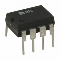
MIC5013BN Micrel Inc, MIC5013BN Datasheet - Page 14

MIC5013BN
Manufacturer Part Number
MIC5013BN
Description
IC DRIVER MOSFET HI/LO SIDE 8IP
Manufacturer
Micrel Inc
Datasheet
1.MIC5013YM.pdf
(15 pages)
Specifications of MIC5013BN
Configuration
High or Low Side
Input Type
Non-Inverting
Delay Time
60µs
Number Of Configurations
1
Number Of Outputs
1
Voltage - Supply
7 V ~ 32 V
Operating Temperature
-40°C ~ 85°C
Mounting Type
Through Hole
Package / Case
8-DIP (0.300", 7.62mm)
Lead Free Status / RoHS Status
Contains lead / RoHS non-compliant
Current - Peak
-
High Side Voltage - Max (bootstrap)
-
Available stocks
Company
Part Number
Manufacturer
Quantity
Price
Company:
Part Number:
MIC5013BN
Manufacturer:
MICREL
Quantity:
5 510
Company:
Part Number:
MIC5013BN
Manufacturer:
SIEMENS
Quantity:
5 510
Part Number:
MIC5013BN
Manufacturer:
MICREL/麦瑞
Quantity:
20 000
MIC5013
Applications Information
Gate Control Circuit
When applying the MIC5010, it is helpful to understand the
operation of the gate control circuitry (see Figure 14). The
gate circuitry can be divided into two sections: 1) charge
pump (oscillator, Q1-Q5, and the capacitors) and 2) gate
turn-off switch (Q6).
When the MIC5010 is in the OFF state, the oscillator is
turned off, thereby disabling the charge pump. Q5 is also
turned off, and Q6 is turned on. Q6 holds the gate pin (G)
at ground potential which effectively turns the external
MOSFET off.
Q6 is turned off when the MIC5013 is commanded on. Q5
pulls the gate up to supply (through 2 diodes). Next, the
charge pump begins supplying current to the gate. The
gate accepts charge until the gate-source voltage reaches
12.5V and is clamped by the zener diode.
A 2-output, three-phase clock switches Q1-Q4, providing a
quasi-tripling action. During the initial phase Q4 and Q2 are
ON. C1 is discharged, and C2 is charged to supply through
MIC5013
O F F
ON
OSCILLATOR
100 kHz
(Continued)
C1
Q2
Q1
Figure 14. Gate Control
125pF
C1
Circuit Detail
14
COM
Q5. For the second phase Q4 turns off and Q3 turns on,
pushing pin C2 above supply (charge is dumped into the
gate). Q3 also charges C1. On the third phase Q2 turns
off and Q1 turns on, pushing the common point of the two
capacitors above supply. Some of the charge in C1 makes
its way to the gate. The sequence is repeated by turning
Q2 and Q4 back on, and Q1 and Q3 off.
In a low-side application operating on a 12 to 15V supply,
the MOSFET is fully enhanced by the action of Q5 alone.
On supplies of more than approximately 14V, current flows
directly from Q5 through the zener diode to ground. To
prevent excessive current flow, the MIC5010 supply should
be limited to 15V in low-side applications.
The action of Q5 makes the MIC5013 operate quickly in
low-side applications. In high-side applications Q5 pre-
charges the MOSFET gate to supply, leaving the charge
pump to carry the gate up to full enhancement 10V above
supply. Bootstrapped high-side drivers are as fast as low-
side drivers since the chip supply is boosted well above
the drain at turn-on.
V
+
Q3
Q4
125pF
C2
C2
Q5
500Ω
Q6
GATE CLAMP
Z E N E R
G
S
12.5V
July 2005
Micrel, Inc.


