IR2132J International Rectifier, IR2132J Datasheet - Page 2
IR2132J
Manufacturer Part Number
IR2132J
Description
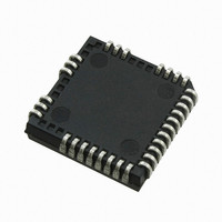
IC DRIVER BRIDGE 3-PHASE 44-PLCC
Manufacturer
International Rectifier
Datasheet
1.IR2132.pdf
(21 pages)
Specifications of IR2132J
Configuration
3 Phase Bridge
Input Type
Inverting
Delay Time
675ns
Current - Peak
250mA
Number Of Configurations
1
Number Of Outputs
3
High Side Voltage - Max (bootstrap)
600V
Voltage - Supply
10 V ~ 20 V
Operating Temperature
-40°C ~ 125°C
Mounting Type
Surface Mount
Package / Case
44-PLCC (32 Leads)
Lead Free Status / RoHS Status
Contains lead / RoHS non-compliant
Other names
*IR2132J
Available stocks
Company
Part Number
Manufacturer
Quantity
Price

Company:
Part Number:
IR2132J
Manufacturer:
International Rectifier
Quantity:
10 000
Part Number:
IR2132J
Manufacturer:
IR
Quantity:
20 000
Company:
Part Number:
IR2132JPBF
Manufacturer:
International Rectifier
Quantity:
10 000
Company:
Part Number:
IR2132JTR
Manufacturer:
International Rectifier
Quantity:
10 000
Part Number:
IR2132JTR
Manufacturer:
IR
Quantity:
20 000
Company:
Part Number:
IR2132JTRPBF
Manufacturer:
International Rectifier
Quantity:
10 000


Absolute Maximum Ratings
Absolute Maximum Ratings indicate sustained limits beyond which damage to the device may occur. All voltage param-
eters are absolute voltages referenced to V
under board mounted and still air conditions. Additional information is shown in Figures 50 through 53.
Recommended Operating Conditions
The Input/Output logic timing diagram is shown in Figure 1. For proper operation the device should be used within the
recommended conditions. All voltage parameters are absolute voltages referenced to V
with all supplies biased at 15V differential. Typical ratings at other bias conditions are shown in Figure 54.
Note 1: Logic operational for V
Symbol
Symbol
V
V
V
V
V
V
V
V
dV
V
V
HO1,2,3
HO1,2,3
LO1,2,3
LO1,2,3
V
V
R
V
V
V
V
V
V
B1,2,3
S1,2,3
B1,2,3
S1,2,3
V
V
P
T
CAO
T
T
CAO
T
CA-
CA-
FLT
FLT
CC
CC
SS
S
SS
IN
IN
A
D
S
L
JA
J
/dt
High Side Floating Supply Voltage
High Side Floating Offset Voltage
High Side Floating Output Voltage
Low Side and Logic Fixed Supply Voltage
Logic Ground
Low Side Output Voltage
Logic Input Voltage (HIN1,2,3 , LIN1,2,3 & ITRIP)
Operational Amplifier Output Voltage
Operational Amplifier Inverting Input Voltage
Allowable Offset Supply Voltage Transient
Package Power Dissipation @ T
Thermal Resistance, Junction to Ambient
Junction Temperature
Storage Temperature
Lead Temperature (Soldering, 10 seconds)
High Side Floating Supply Voltage
High Side Floating Offset Voltage
High Side Floating Output Voltage
Low Side and Logic Fixed Supply Voltage
Logic Ground
Low Side Output Voltage
Logic Input Voltage (HIN1,2,3 , LIN1,2,3 & ITRIP)
Operational Amplifier Output Voltage
Operational Amplifier Inverting Input Voltage
Ambient Temperature
FAULT Output Voltage
FAULT Output Voltage
S
of (V
Parameter
Parameter
S0
- 5V) to (V
Definition
Definition
S0
. The Thermal Resistance and Power Dissipation ratings are measured
A
S0
+25°C
+ 600V). Logic state held for V
(44 Lead PLCC)
(44 Lead PLCC)
(28 Lead SOIC)
(28 Lead SOIC)
(28 Lead DIP)
(28 Lead DIP)
V
V
V
V
V
V
V
S1,2,3
V
S1,2,3
B1,2,3
Note 1
V
SS
SS
SS
SS
CC
Min.
Min.
S
-0.3
-0.3
S0
V
V
V
V
-0.3
S1,2,3
-55
-40
10
—
—
—
—
—
—
—
—
—
-5
0
of (V
SS
SS
SS
SS
- 0.3
- 0.3
- 0.3
- 0.3
- 25
. The V
- 0.3
+ 10
- 25
Value
Value
S0
S
- 5V) to (V
V
V
offset rating is tested
V
V
V
V
V
V
V
B1,2,3
B1,2,3
S1,2,3
V
CC
CC
CC
CC
CC
CC
V
Max.
Max.
SS
V
V
525
150
150
300
600
B1,2,3
125
1.5
1.6
2.0
25
50
83
78
63
20
5
CC
CC
5
5
+ 0.3
+ 0.3
+ 0.3
+ 0.3
+ 0.3
+ 0.3
+ 5
+ 0.3
+ 0.3
+ 20
S0
- V
BS
Units
Units
°C/W
V/ns
).
°C
°C
V
W
V
Related parts for IR2132J
Image
Part Number
Description
Manufacturer
Datasheet
Request
R

Part Number:
Description:
SCHOTTKY RECTIFIER
Manufacturer:
International Rectifier Corp.
Datasheet:
Part Number:
Description:
SCHOTTKY RECTIFIER
Manufacturer:
International Rectifier Corp.
Datasheet:
Part Number:
Description:
SCHOTTKY RECTIFIER
Manufacturer:
International Rectifier Corp.
Datasheet:
Part Number:
Description:
SCHOTTKY RECTIFIER
Manufacturer:
International Rectifier Corp.
Datasheet:
Part Number:
Description:
SCHOTTKY RECTIFIER
Manufacturer:
International Rectifier Corp.
Datasheet:
Part Number:
Description:
SCHOTTKY RECTIFIER
Manufacturer:
International Rectifier Corp.
Datasheet:
Part Number:
Description:
SCHOTTKY RECTIFIER
Manufacturer:
International Rectifier Corp.
Datasheet:
Part Number:
Description:
SCHOTTKY RECTIFIER
Manufacturer:
International Rectifier Corp.
Datasheet:
Part Number:
Description:
SCHOTTKY RECTIFIER
Manufacturer:
International Rectifier Corp.
Datasheet:
Part Number:
Description:
SCHOTTKY RECTIFIER
Manufacturer:
International Rectifier Corp.
Datasheet:
Part Number:
Description:
SCHOTTKY RECTIFIER
Manufacturer:
International Rectifier Corp.
Datasheet:
Part Number:
Description:
SCHOTTKY RECTIFIER
Manufacturer:
International Rectifier Corp.
Datasheet:
Part Number:
Description:
SCHOTTKY RECTIFIER
Manufacturer:
International Rectifier Corp.
Datasheet:
Part Number:
Description:
SCHOTTKY RECTIFIER
Manufacturer:
International Rectifier Corp.
Datasheet:
Part Number:
Description:
SCHOTTKY RECTIFIER
Manufacturer:
International Rectifier Corp.
Datasheet: