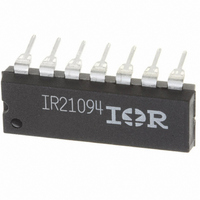
IR21094 International Rectifier, IR21094 Datasheet

IR21094
Specifications of IR21094
Available stocks
Related parts for IR21094
IR21094 Summary of contents
Page 1
... This/These diagram(s) show electrical connections only. Please refer to our Application Notes and DesignTips for proper circuit board layout. www.irf.com IR2109(4) HALF-BRIDGE DRIVER Product Summary V OFFSET on/off Dead Time (programmable up to 5uS for IR21094) resistor (IR21094) Packages 8 Lead SOIC up to 600V TO LOAD ...
Page 2
... High side floating supply offset voltage S V High side floating output voltage HO V Low side and logic fixed supply voltage CC V Low side output voltage LO DT Programmable dead-time pin voltage (IR21094 only) V Logic input voltage (IN & SD Logic ground (IR21094/IR21894 only /dt Allowable offset supply voltage transient S P ...
Page 3
... V Low side and logic fixed supply voltage CC V Low side output voltage LO V Logic input voltage (IN & SD Programmable dead-time pin voltage (IR21094 only) V Logic ground (IR21094 only Ambient temperature A Note 1: Logic operational for +600V. Logic state held for V S DT97-3 for more details). ...
Page 4
IR2109 ( & (PbF) S Static Electrical Characteristics 15V COM, DT= V BIAS parameters are referenced to V /COM and are applicable to the respective ...
Page 5
... Functional Block Diagrams IR2109 IN DEADTIME +5V SD IR21094 IN DT DEADTIME +5V SD VSS www.irf.com IR2109 ( PULSE HV FILTER LEVEL SHIFTER VSS/COM LEVEL PULSE SHIFT GENERATOR VSS/COM LEVEL DELAY SHIFT PULSE HV FILTER LEVEL SHIFTER VSS/COM LEVEL PULSE SHIFT GENERATOR VSS/COM LEVEL DELAY SHIFT ) & (PbF) ...
Page 6
... Logic input for high and low side gate driver outputs (HO and LO), in phase with HO (referenced to COM for IR2109 and VSS for IR21094) Logic input for shutdown (referenced Programmable dead-time lead, referenced to VSS. (IR21094 only) VSS Logic Ground (21094 only) V High side floating supply ...
Page 7
Figure 1. Input/Output Timing Diagram SD 50 90% LO Figure 3. Shutdown Waveform Definitions IN (LO) 50% 50% IN (HO 10% MT 90% LO Figure 5. Delay Matching Waveform Definitions www.irf.com ...
Page 8
IR2109 ( & (PbF) S 1300 1100 900 700 T yp. 500 -50 - Temperature ( Figure 6A. Turn-on Propagation Delay vs. Temperature 500 400 300 Ma x. 200 T ...
Page 9
Max. 200 T yp. 100 0 -50 - Temperature ( Figure 8A. SD Propagation Delay vs. Temperature 500 400 300 200 Max. T yp. 100 - ...
Page 10
IR2109 ( & (PbF) S 200 150 100 yp. 0 -50 - Temperature ( o Figure 10A. Turn-off Fall Time vs. Temperature 1000 800 Ma x. 600 T yp. ...
Page 11
... R (K Ω Figure 11C. Deadtime vs (IR21094 only Supply Voltage (V) CC Figure 12B. Logic “1” Input Voltage vs. Supply Voltage www.irf.com IR2109 ( ax. T yp. Max in 150 200 -50 -25 Figure 12A. Logic “1” Input Voltage Min -50 -25 Figure 13A. Logic “0” Input Voltage ) & ...
Page 12
IR2109 ( & (PbF Min Supply Voltage (V) CC Figure 13B. Logic “0” Input Current vs. Supply Voltage ...
Page 13
Min Supply Voltage (V) CC Figure 15B. SD Negative Going Threshold vs. Supply Volta 4 3 Max yp Supply Voltage ...
Page 14
IR2109 ( & (PbF) S 1.5 1.2 0 0.6 T yp. 0 Supply Voltage (V) BIAS Figure 17B. Low Level Output Voltage vs. Supply Voltage 500 400 300 ...
Page 15
Max . 100 T yp. Min Supply Voltage (V) BS Figure 19B Supply Current ge vs. Supply Volta 3.0 2.5 2.0 1.5 Max. 1.0 T yp. 0.5 Min. 0.0 ...
Page 16
IR2109 ( & (PbF Max yp Supply Voltage (V) CC Figure 21B. Logic “1” Input Current vs. Supply Voltage ...
Page 17
Max yp. 8 Min -50 - Temperature ( o C) Figure 24 Undervoltage Threshold (-) vs. Temperature 11 10 Max yp. 8 Min -50 -25 ...
Page 18
IR2109 ( & (PbF) S 500 400 300 200 T yp. 100 Min Supply Voltage (V) BIAS Figure 27B. Output Source Current vs. Supply Voltage 600 500 400 300 T ...
Page 19
Frequency (KHz) Figure 30. IR2109 vs Frequency (IRFBC20) R gate = 33W 15V 140 120 100 Frequency (KHz) Figure 32. IR2109 ...
Page 20
... Figure 35. IR21094 vs. Frequency (IRFBC30), 140 120 100 140V 80 70V 100 1000 Figure 37. IR21094 vs. Frequency (IRFPE50), 140V 70V 0V 10 100 1000 Frequency (KHz =15V gate CC 140V 70V 0V 10 100 1000 Frequency (KHz =15V gate CC www.irf.com ...
Page 21
Frequency (KHz) Figure 38. IR2109S vs. Frequency (IRFBC20 =15V gate CC 140 120 100 Frequency (KHz) Figure 40. IR2109S vs. ...
Page 22
... Figure 43. IR21094S vs. Frequency (IRFBC30), 140 120 100 140V 80 70V 100 1000 Figure 45. IR21094S vs. Frequency (IRFPE50), 140V 70V 0V 10 100 1000 Frequency (KHz =15V gate CC 140V 70V 0V 10 100 1000 Frequency (KHz =15V gate CC www.irf.com ...
Page 23
Case Outlines 0.25 [.010 0.25 [.010 NOT DIMENSIONING & TOLE RANCING PER AS ...
Page 24
IR2109 ( & (PbF Lead PDIP 14 Lead SOIC (narrow body) Data and specifications subject to change without notice. 7/11/2003 01-6010 01-3002 03 (MS-001AC) 01-6019 01-3063 00 (MS-012AB) www.irf.com ...
Page 25
... Lead-Free Part 8-Lead PDIP IR2109 8-Lead SOIC IR2109S 14-Lead PDIP IR21094 14-Lead SOIC IR21094S order IR21094SPbF This product has been designed and qualified for the Industrial market. Qualification Standards can be found on IR’s Website. Data and specifications subject to change without notice. ...


