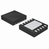
NCP5359MNR2G ON Semiconductor, NCP5359MNR2G Datasheet - Page 5

NCP5359MNR2G
Manufacturer Part Number
NCP5359MNR2G
Description
IC GATE DRIVER VR11.1/AMD 10DFN
Manufacturer
ON Semiconductor
Type
High Side/Low Sider
Datasheet
1.NCP5359MNR2G.pdf
(9 pages)
Specifications of NCP5359MNR2G
Configuration
High and Low Side, Synchronous
Input Type
PWM
Delay Time
10.0ns
Number Of Configurations
1
Number Of Outputs
2
High Side Voltage - Max (bootstrap)
35V
Voltage - Supply
10 V ~ 13.2 V
Operating Temperature
0°C ~ 85°C
Mounting Type
Surface Mount
Package / Case
10-VFDFN Exposed Pad
Product
Driver ICs - Various
Rise Time
16 ns
Supply Voltage (min)
10 V
Maximum Operating Temperature
+ 85 C
Mounting Style
SMD/SMT
Minimum Operating Temperature
0 C
Number Of Drivers
2
Lead Free Status / RoHS Status
Lead free / RoHS Compliant
Current - Peak
-
Lead Free Status / Rohs Status
Lead free / RoHS Compliant
5. Guaranteed by design; not tested in production .
6. For propagation delays, ”t
7. Design guaranteed.
ELECTRICAL CHARACTERISTICS
Supply Voltage
Supply Current
Undervoltage Lockout
V
V
Output Overvoltage Trip Threshold at
Startup
EN Input
PWM Input
High Side Driver
Low Side Driver
Thermal Shutdown
V
Power ON Reset threshold
V
Normal Operation
V
BST Quiescent Supply Current in
Normal Operation
BST Standby Current
Input Voltage High
Input Voltage Low
Hysteresis (Note 5)
Enable Pin Sink Current
Propagation Delay Time (Note 5)
DRVH Comparator Drop Threshold
PWM Input Self Bias Voltage
DRVL Comparator Rise Threshold
Input Current
Output Resistance, Sourcing
Output Resistance, Sinking
Transition Time (Note 7)
Propagation Delay (Notes 5 & 6)
Output Resistance, Sourcing
Output Resistance, Sinking
Transition Time (Note 7)
Propagation Delay (Notes 5 & 6)
Negative Current Detector Threshold
Thermal Shutdown
Thermal Shutdown Hysteresis
CC
CC
CC
CC
CC
Start Threshold
UVLO Hysteresis
Operating Voltage
Quiescent Supply Current in
Standby Current
Characteristics
pdh
” refers to the specified signal going high ”t
(V
I
I
VTH_DRVH
VTH_DRVL
I
BST1_normal
BST2_normal
VCC_NORM
tpdh
I
V
tpdh
V
I
I
VCC
I
tpdl
tpdl
Symbol
VCC_SBC
OVPSU
CC
BST1_SD
BST2_SD
VCC
EN_SINK
V
tpd
R
tr
R
V
EN_LOW
R
tf
R
tr
Tsd
EN_HYS
tpd
V
tf
V
I
V
EN_HI
PWM
DRVH
DRVH
DRVL
DRVL
NCDT
Tsd
H_TG
H_BG
PWM
L_TG
L_BG
POR
DRVH
CC
DRVL
= 12 V, T
DRVH
hEN
DRVL
lEN
hys
HYS
TH
A
EN = 5 V, PWM = OSC, F
C
EN = GND; No switching
PWM = +5 V, SW = 0 V
PWM = GND, SW = 0 V
PWM = +5 V
PWM = GND
Power Startup time, V
(Without trimming)
V
PWM = 0 V, EN = GND
V
V
C
C
Driving High, C
Driving Low, C
SW = GND
SW = V
C
C
Driving High, C
Driving Low, C
(Note 7)
(Note 7)
(Note 7)
= 0°C to +85°C, V
http://onsemi.com
LOAD
CC
BST
BST
LOAD
LOAD
LOAD
LOAD
= 5.5 V
– V
– V
= 0 p
= 3 nF, V
= 3 nF, V
= 3 nF
= 3 nF
CC
SW
SW
Test Conditions
5
= 12 V
= 12 V
LOAD
LOAD
LOAD
LOAD
BST
BST
pdl
EN
” refers to it going low.
= 3 nF
= 3 nF
– V
– V
= 3 nF
= 3 nF
= 5 V unless otherwise noted)
CC
SW
SW
> 9 V.
SW
= 12 V
= 12 V
= 100 k
Min
150
8.2
1.8
2.0
5.0
2.2
1.4
8.0
8.0
10
10
10
0.25
0.25
−1.0
Typ
500
170
2.8
2.0
0.5
1.0
1.0
8.7
1.0
1.5
2.0
1.0
2.0
1.0
20
20
30
16
16
20
11
11
Max
13.2
5.0
1.0
1.8
1.8
9.5
2.0
1.0
1.6
0.8
3.5
2.5
3.5
2.5
60
60
25
15
35
30
25
15
35
30
Units
mA
mA
mA
mA
mV
mA
mV
mA
°C
°C
ns
ns
ns
ns
ns
ns
V
V
V
V
V
V
V
V
V
V
W
W
W
W


