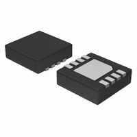
NCP3420MNR2G ON Semiconductor, NCP3420MNR2G Datasheet - Page 2

NCP3420MNR2G
Manufacturer Part Number
NCP3420MNR2G
Description
MOSFET DVR DUAL 1PH 12V 8-DFN
Manufacturer
ON Semiconductor
Datasheet
1.NCP3420MNR2G.pdf
(9 pages)
Specifications of NCP3420MNR2G
Configuration
High and Low Side, Synchronous
Input Type
Non-Inverting
Delay Time
30ns
Number Of Configurations
1
Number Of Outputs
2
High Side Voltage - Max (bootstrap)
12V
Voltage - Supply
4.6 V ~ 13.2 V
Operating Temperature
0°C ~ 85°C
Mounting Type
Surface Mount
Package / Case
8-TFDFN Exposed Pad
Lead Free Status / RoHS Status
Lead free / RoHS Compliant
Current - Peak
-
Lead Free Status / Rohs Status
Lead free / RoHS Compliant
PIN DESCRIPTION
SO−8
OD
1
2
3
4
5
6
7
8
IN
3
2
DFN8
1
2
3
4
5
6
7
8
V
CC
START
Symbol
PGND
DRVH
DRVL
OFF TIMER
SWN
BST
V
MIN DRVL
OD
IN
CC
UVLO
TSD
STOP
Upper MOSFET Floating Bootstrap Supply. A capacitor connected between BST and SW pins holds
this bootstrap voltage for the high−side MOSFET as it is switched. The recommended capacitor value
is between 100 nF and 1.0 mF. An external diode is required with the NCP3420.
Logic−Level Input. This pin has primary control of the drive outputs.
Output Disable. When low, normal operation is disabled forcing DRVH and DRVL low.
Input Supply. A 1.0 mF ceramic capacitor should be connected from this pin to PGND.
Output drive for the lower MOSFET.
Power Ground. Should be closely connected to the source of the lower MOSFET.
Switch Node. Connect to the source of the upper MOSFET.
Output drive for the upper MOSFET.
Figure 1. Block Diagram
http://onsemi.com
2
NON−OVERLAP
FALLING
FALLING
TIMERS
DELAY
DELAY
EDGE
EDGE
Description
MONITOR
MONITOR
1
8
7
4
5
6
V
BST
DRVH
SWN
DRVL
PGND
CC


