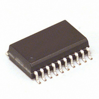
MCZ33883EG Freescale Semiconductor, MCZ33883EG Datasheet - Page 16

MCZ33883EG
Manufacturer Part Number
MCZ33883EG
Description
IC PRE-DRIVER FULL BRIDGE 20SOIC
Manufacturer
Freescale Semiconductor
Type
High Side/Low Sider
Datasheet
1.MCZ33883EGR2.pdf
(21 pages)
Specifications of MCZ33883EG
Configuration
H Bridge
Input Type
Non-Inverting
Delay Time
200ns
Current - Peak
2A
Number Of Configurations
1
Number Of Outputs
4
Voltage - Supply
5.5 V ~ 55 V
Operating Temperature
-40°C ~ 125°C
Mounting Type
Surface Mount
Package / Case
20-SOIC (7.5mm Width)
Rise Time
180 ns
Fall Time
180 ns
Supply Voltage (min)
5.5 V
Supply Current
2.2 mA
Maximum Power Dissipation
1250 mW
Maximum Operating Temperature
+ 125 C
Mounting Style
SMD/SMT
Bridge Type
H Bridge
Minimum Operating Temperature
- 40 C
Number Of Drivers
4
Lead Free Status / RoHS Status
Lead free / RoHS Compliant
High Side Voltage - Max (bootstrap)
-
Lead Free Status / Rohs Status
Lead free / RoHS Compliant
Available stocks
Company
Part Number
Manufacturer
Quantity
Price
Part Number:
MCZ33883EG
Manufacturer:
FREESCALE
Quantity:
20 000
Company:
Part Number:
MCZ33883EGR2
Manufacturer:
FREESCALE
Quantity:
1 490
Part Number:
MCZ33883EGR2
Manufacturer:
FREESCALE
Quantity:
20 000
GATE PROTECTION
regulator. The high-side driver is supplied from the internal
charge pump buffered at CP_OUT.
regulator, which ensures that V
maximum V
pump, the voltage at CP_OUT can be up to 65 V. The high-
side gate is clamped internally in order to avoid a V
exceeding 18 V.
that protects the driver and the external MOSFET from a fly-
back voltage that can occur when driving inductive load. This
fly-back voltage can reach high negative voltage values and
needs to be clamped externally, as shown in
16
33883
FUNCTIONAL DEVICE OPERATION
PROTECTION AND DIAGNOSTIC FEATURES
Figure 12. Gate Protection and Flyback Voltage Clamp
The low-side driver is supplied from the built-in low-drop
The low-side gate is protected by the internal linear
Gate protection does not include a fly-back voltage clamp
LR_OUT
IN
IN
GS
Output
Output
Driver
Driver
. Especially when working with the charge
CP_OUT
OUT
OUT
GATE_HS
SRC_HS
GATE_LS
D
c l
GATE_LS
M
M
PROTECTION AND DIAGNOSTIC FEATURES
1
2
does not exceed the
L
1
Flyback Voltage
Figure
V
Inductive
Conditions
Under All
Clamp
GS
GS
V
< 14 V
12.
CC
LOAD DUMP AND REVERSE BATTERY
double battery of 24 V. Protection against reverse polarity is
ensured by the external power MOSFET with the free-
wheeling diodes forming a conducting pass from ground to
V
To protect the circuit an external diode can be put on the
battery line. It is not recommended putting the diode on the
ground line.
TEMPERATURE PROTECTION
bridge. Temperature shutdown protects the circuitry against
temperature damage by switching off the output drivers. Its
typical value is 175°C with an hysteresis of 15°C.
DV/DT AT V
a diode drop voltage) to avoid perturbation of the high-side
driver.
sudden changes at V
flowing through terminal C1, as shown in
of the minimum peak current, I
a t
current, I
600 ns. Current sourced by terminal C1 during a large dV / dt
will result in a negative voltage at terminal C1
The minimum peak voltage V
duration of t
pump capacitor (Ccp) capacitor can be added in order to limit
the surge current.
CC
C1
V
There is temperature shutdown protection per each half-
V
In some applications a large dV / dt at terminal C2 owing to
For positive transitions at terminal C2, the absolute value
For negative transitions at terminal C2, the maximum peak
CC
. Additional protection is not provided within the circuit.
CC
min duration of 600 ns.
and V
voltage must be higher than (SRC_HS voltage minus
C1
max, is specified at 2.0 A for a t
C1
CC2
CC
max = 600 ns. A series resistor with the charge
can sustain load a dump pulse of 40 V and
CC
Analog Integrated Circuit Device Data
can cause large peak currents
C1
C1
min is specified at -1.5 V for a
min, is specified at 2.0 A for
Freescale Semiconductor
Figure
C1
max duration of
(Figure
13.
13).


