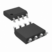
LM2724M National Semiconductor, LM2724M Datasheet - Page 4

LM2724M
Manufacturer Part Number
LM2724M
Description
IC DRIVER MOSFET DUAL SYNC 8SOIC
Manufacturer
National Semiconductor
Datasheet
1.LM2724LD.pdf
(8 pages)
Specifications of LM2724M
Configuration
High and Low Side, Synchronous
Input Type
Non-Inverting
Delay Time
19ns
Current - Peak
3A
Number Of Configurations
1
Number Of Outputs
2
High Side Voltage - Max (bootstrap)
28V
Voltage - Supply
4.3 V ~ 6.8 V
Operating Temperature
-40°C ~ 125°C
Mounting Type
Surface Mount
Package / Case
8-SOIC (3.9mm Width)
Lead Free Status / RoHS Status
Lead free / RoHS Compliant
Other names
*LM2724M
Available stocks
Company
Part Number
Manufacturer
Quantity
Price
Part Number:
LM2724M
Manufacturer:
NS/国半
Quantity:
20 000
Part Number:
LM2724MX
Manufacturer:
NS/国半
Quantity:
20 000
www.national.com
POWER SUPPLY
I
TOP DRIVER
t
t
t
t
BOTTOM DRIVER
t
t
t
t
LOGIC
V
V
V
V
V
I
q_op
4
6
3
5
8
2
7
1
leak_SYNC
Absolute Maximum Ratings
If Military/Aerospace specified devices are required,
please contact the National Semiconductor Sales Office/
Distributors for availability and specifications.
Electrical Characteristics
LM2724A
V
T
uvlo_up
uvlo_dn
uvlo_hys
IH_SYNC
IL_SYNC
V
BOOT to SW
BOOT to GND (Note 2)
SW to GND
Junction Temperature
Power Dissipation
(Note 3)
CC
A
CC
Symbol
= T
= BOOT = SYNC = 5V, SW = GND = 0V, unless otherwise specified. Typicals and limits appearing in plain type apply for
J
= +25˚C. Limits appearing in boldface type apply over the entire operating temperature range.
Operating Quiescent
Current
Peak Pull-Up Current
Pull-Up Rds_on
Peak Pull-down Current
Pull-down Rds_on
Rise Time
Fall Time
Pull-Up Dead Time
Pull-Down Delay
Peak Pull-Up Current
Pull-up Rds_on
Peak Pull-down Current
Pull-down Rds_on
Rise Time
Fall Time
Pull-up Dead Time
Pull-down Delay
V
Under-Voltage-Lock-Out
Upper Threshold
V
Under-Voltage-Lock-Out
Lower Threshold
V
Under-Voltage-Lock-Out
Hysteresis
SYNC Pin High Input
SYNC Pin Low Input
SYNC Pin Leakage
Current
CC
CC
CC
Parameter
720mW (SO-8)
3.2W (LLP-8)
Condition
IN = 0V
I
I
Timing Diagram, C
3.3nF
Timing Diagram
Timing Diagram, from IN
Falling Edge
I
I
Timing Diagram, C
3.3nF
Timing Diagram
Timing Diagram
V
5V
VCC falls from 5V toward
0V
V
SYNC = 5V, Sink Current
SYNC = 0V, Source Current
BOOT
SW
VCC
GND
(Note 1)
CC
CC
= I
+150˚C
rises from 0V toward
falls from 5V toward 0V
= I
= I
= I
HG
35V
30V
LG
LG
7V
7V
HG
= 0.3A
= 0.3A
= 0.3A
= 0.3A
4
LOAD
LOAD
Operating Ratings
Storage Temperature
ESD Susceptibility
Soldering Time, Temperature
V
Junction Temperature Range
CC
Human Body Model (Note 4)
=
=
55%
Min
2.5
−3.2
Typ
145
3.0
1.2
0.5
3.2
1.1
3.2
0.6
0.8
17
12
19
27
17
14
22
13
(Note 1)
Max
25%
195
10
−65˚C to 150˚C
4
2
-40˚C to 125˚C
10sec., 300˚C
4.3V to 6.8V
2.0 kV
Units
V
µA
µA
ns
ns
ns
ns
ns
ns
ns
ns
Ω
Ω
Ω
Ω
A
A
A
A
V
V
V
CC


