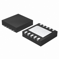
ISL6622AIRZ Intersil, ISL6622AIRZ Datasheet - Page 8

ISL6622AIRZ
Manufacturer Part Number
ISL6622AIRZ
Description
IC MOSFET DRVR SYNC BUCK 10-DFN
Manufacturer
Intersil
Datasheet
1.ISL6622AIRZ.pdf
(11 pages)
Specifications of ISL6622AIRZ
Configuration
High and Low Side, Synchronous
Input Type
PWM
Delay Time
20ns
Current - Peak
1.25A
Number Of Configurations
1
Number Of Outputs
2
High Side Voltage - Max (bootstrap)
36V
Voltage - Supply
6.8 V ~ 13.2 V
Operating Temperature
-40°C ~ 85°C
Mounting Type
Surface Mount
Package / Case
10-DFN
Lead Free Status / RoHS Status
Lead free / RoHS Compliant
The total gate drive power losses are dissipated among the
resistive components along the transition path, as outlined in
Equation 4. The drive resistance dissipates a portion of the
total gate drive power losses, the rest will be dissipated by the
external gate resistors (R
resistors (R
the typical upper and lower gate drives turn-on current path.
Application Information
Layout Considerations
During switching of the devices, the parasitic inductances of
the PCB and the power devices’ packaging (both upper and
lower MOSFETs) leads to ringing, possibly in excess of the
absolute maximum rating of the devices. Careful layout can
help minimize such unwanted stress. The following advice is
meant to lead to an optimized layout:
• Keep decoupling loops (LVCC-GND and BOOT-PHASE)
P
P
P
R
DR
DR_UP
DR_LOW
EXT1
FIGURE 4. TYPICAL LOWER-GATE DRIVE TURN-ON PATH
as short as possible.
FIGURE 3. TYPICAL UPPER-GATE DRIVE TURN-ON PATH
UVCC
=
LVCC
P
=
DR_UP
=
R
=
GI1
⎛
⎜
⎝
PHASE
G1
--------------------------------------
R
⎛
⎜
⎝
HI1
--------------------------------------
R
R
R
+
BOOT
and R
LO2
HI2
R
HI2
R
+
R
-------------
R
N
LO1
HI1
+
P
GI1
HI1
Q1
R
R
+
DR_LOW
HI2
EXT1
R
GI2
EXT2
) of MOSFETs. Figures 3 and 4 show
G1
+
+
+
--------------------------------------- -
R
and R
I
LO1
--------------------------------------- -
R
Q
R
R
8
LO2
G2
EXT2
R
•
R
G
G1
VCC
+
LO1
R
G
G2
+
R
LO2
R
C
EXT1
R
GI2
) and the internal gate
GD
=
R
C
EXT2
C
GI1
GD
R
GS
C
G2
GS
⎞
⎟
⎠
•
⎞
⎟
⎠
S
+
P
---------------------
•
S
R
-------------
Qg_Q1
N
P
---------------------
GI2
Q2
Qg_Q2
2
D
2
D
Q2
C
Q1
DS
C
(EQ. 4)
DS
ISL6622A
• Minimize trace inductance, especially low-impedance
• Minimize the inductance of the PHASE node: ideally, the
• Minimize the input current loop: connect the source of the
In addition, for improved heat dissipation, place copper
underneath the IC whether it has an exposed pad or not. The
copper area can be extended beyond the bottom area of the
IC and/or connected to buried power ground plane(s) with
thermal vias. This combination of vias for vertical heat
escape, extended surface copper islands, and buried planes
combine to allow the IC and the power switches to achieve
their full thermal potential.
Upper MOSFET Self Turn-On Effects At Startup
Should the driver have insufficient bias voltage applied, its
outputs are floating. If the input bus is energized at a high
dV/dt rate while the driver outputs are floating, due to
self-coupling via the internal C
the upper MOSFET could momentarily rise up to a level
greater than the threshold voltage of the device, potentially
turning on the upper switch. Therefore, if such a situation
could conceivably be encountered, it is a common practice to
place a resistor (R
upper MOSFET to suppress the Miller coupling effect. The
value of the resistor depends mainly on the input voltage’s
rate of rise, the C
threshold of the upper MOSFET. A higher dV/dt, a lower
C
will require a smaller resistor to diminish the effect of the
internal capacitive coupling. For most applications, the
integrated 20kΩ resistor is sufficient, not affecting normal
performance and efficiency.
The coupling effect can be roughly estimated with
Equation 5, which assumes a fixed linear input ramp and
neglects the clamping effect of the body diode of the upper
drive and the bootstrap capacitor. Other parasitic
components such as lead inductances and PCB
capacitances, are also not taken into account. Figure 5
provides a visual reference for this phenomenon and its
potential solution.
V
R
DS
GS_MILLER
lines: all power traces (UGATE, PHASE, LGATE, GND,
LVCC) should be short and wide, as much as possible.
source of the upper and the drain of the lower MOSFET
should be as close as thermally allowable.
lower MOSFET to ground as close to the transistor pin as
feasible; input capacitors (especially ceramic decoupling)
should be placed as close to the drain of upper and source
of lower MOSFETs as possible.
=
/C
R
GS
UGPH
ratio, and a lower gate-source threshold upper FET
=
+
R
dV
------ - R C
dt
GI
GD
UGPH
⋅
/C
⋅
GS
C
) across the gate and source of the
rss
rss
ratio, as well as the gate-source
⎛
⎜
⎜
⎜
⎜
⎝
1 e
=
–
GD
C
--------------------------------- -
dV
------ - R C
GD
dt
of the MOSFET, the gate of
–
⋅
V
DS
⋅ iss
C
⎞
⎟
⎟
⎟
⎟
⎠
iss
=
C
GD
March 19, 2009
+
(EQ. 5)
FN6601.2
C
GS


