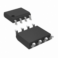
LM5100AMX/NOPB National Semiconductor, LM5100AMX/NOPB Datasheet - Page 12

LM5100AMX/NOPB
Manufacturer Part Number
LM5100AMX/NOPB
Description
IC DVR HALF-BRIDGE HV 8-SOIC
Manufacturer
National Semiconductor
Datasheet
1.LM5101CSDNOPB.pdf
(18 pages)
Specifications of LM5100AMX/NOPB
Configuration
High and Low Side, Synchronous
Input Type
Non-Inverting
Delay Time
20ns
Current - Peak
3A
Number Of Configurations
1
Number Of Outputs
2
High Side Voltage - Max (bootstrap)
118V
Voltage - Supply
9 V ~ 14 V
Operating Temperature
-40°C ~ 125°C
Mounting Type
Surface Mount
Package / Case
8-SOIC (3.9mm Width)
Number Of Drivers
2
Driver Configuration
Non-Inverting
Driver Type
High and Low Side
Input Logic Level
CMOS
Rise Time
430ns
Fall Time
260ns
Propagation Delay Time
20ns
Operating Supply Voltage (max)
14V
Peak Output Current
3mA
Operating Supply Voltage (min)
9V
Turn Off Delay Time
1ns
Turn On Delay Time (max)
1ns
Operating Temp Range
-40C to 125C
Operating Temperature Classification
Automotive
Mounting
Surface Mount
Pin Count
8
Package Type
SOIC N
Lead Free Status / RoHS Status
Lead free / RoHS Compliant
Other names
LM5100AMX
Available stocks
Company
Part Number
Manufacturer
Quantity
Price
Company:
Part Number:
LM5100AMX/NOPB
Manufacturer:
ROHM
Quantity:
6 262
Part Number:
LM5100AMX/NOPB
Manufacturer:
TI/德州仪器
Quantity:
20 000
www.national.com
Layout Considerations
The optimum performance of high and low-side gate drivers
cannot be achieved without taking due considerations during
circuit board layout. Following points are emphasized.
1.
2.
3.
4.
Low ESR / ESL capacitors must be connected close to
the IC, between VDD and VSS pins and between the HB
and HS pins to support the high peak currents being
drawn from VDD during turn-on of the external MOSFET.
To prevent large voltage transients at the drain of the top
MOSFET, a low ESR electrolytic capacitor must be
connected between MOSFET drain and ground (VSS).
In order to avoid large negative transients on the switch
node (HS pin), the parasitic inductances in the source of
top MOSFET and in the drain of the bottom MOSFET
(synchronous rectifier) must be minimized.
Grounding Considerations:
is to confine the high peak currents that charge and
a) The first priority in designing grounding connections
12
A recommended layout pattern for the driver is shown in the
following figure. If possible a single layer placement is pre-
ferred.
discharge the MOSFET gate into a minimal physical
area. This will decrease the loop inductance and
minimize noise issues on the gate terminal of the
MOSFET. The MOSFETs should be placed as close as
possible to the gate driver.
capacitor, the bootstrap diode, the local ground
referenced bypass capacitor and low-side MOSFET
body diode. The bootstrap capacitor is recharged on a
cycle-by-cycle basis through the bootstrap diode from
the ground referenced VDD bypass capacitor. The
recharging occurs in a short time interval and involves
high peak current. Minimizing this loop length and area
on the circuit board is important to ensure reliable
operation.
b) The second high current path includes the bootstrap
20203138


