LM27222M/NOPB National Semiconductor, LM27222M/NOPB Datasheet
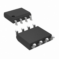
IC MOSFET DVR SYNC 4.5A HS 8SOIC

LM27222M/NOPB

Manufacturer Part Number
LM27222M/NOPB
Description
IC MOSFET DVR SYNC 4.5A HS 8SOIC
Manufacturer
National Semiconductor
Datasheet

Specifications of LM27222M/NOPB

Configuration
High and Low Side, Synchronous
Input Type
PWM
Delay Time
14ns
Current - Peak
3A
Number Of Configurations
1
Number Of Outputs
2
High Side Voltage - Max (bootstrap)
30V
Voltage - Supply
4 V ~ 6.85 V
Operating Temperature
-40°C ~ 125°C
Mounting Type
Surface Mount
Package / Case
8-SOIC (3.9mm Width)
Number Of Drivers
2
Driver Configuration
Invert/Non-Invert
Driver Type
High and Low Side
Rise Time
17ns
Fall Time
14ns
Propagation Delay Time
8ns
Operating Supply Voltage (max)
6.85V
Peak Output Current
4.5mA
Power Dissipation
720mW
Operating Supply Voltage (min)
4V
Operating Temp Range
-40C to 125C
Operating Temperature Classification
Automotive
Mounting
Surface Mount
Pin Count
8
Package Type
SOIC N
Lead Free Status / RoHS Status
Lead free / RoHS Compliant
Other names
LM27222M
© 2006 National Semiconductor Corporation
LM27222
High-Speed 4.5A Synchronous MOSFET Driver
General Description
The LM27222 is a dual N-channel MOSFET driver designed
to drive MOSFETs in push-pull configurations as typically
used in synchronous buck regulators. The LM27222 takes
the PWM output from a controller and provides the proper
timing and drive levels to the power stage MOSFETs. Adap-
tive shoot-through protection prevents damaging and effi-
ciency reducing shoot-through currents, thus ensuring a ro-
bust design capable of being used with nearly any MOSFET.
The adaptive shoot-through protection circuitry also reduces
the dead time down to as low as 10ns, ensuring the highest
operating efficiency. The peak sourcing and sinking current
for each driver of the LM27222 is about 3A and 4.5Amps
respectively with a Vgs of 5V. System performance is also
enhanced by keeping propagation delays down to 8ns. Effi-
ciency is once again improved at all load currents by sup-
porting synchronous, non-synchronous, and diode emulation
modes through the LEN pin. The minimum output pulse
width realized at the output of the MOSFETs is as low as
30ns. This enables high operating frequencies at very high
conversion ratios in buck regulator designs. To support low
power states in notebook systems, the LM27222 draws only
5µA from the 5V rail when the IN and LEN inputs are low or
floating.
Typical Application
DS201179
FIGURE 1.
Features
n Adaptive shoot-through protection
n 10ns dead time
n 8ns propagation delay
n 30ns minimum on-time
n 0.4Ω pull-down and 0.9Ω pull-up drivers
n 4.5A peak driving current
n MOSFET tolerant design
n 5µA quiescent current
n 30V maximum input voltage in buck configuration
n 4V to 6.85V operating voltage
n SO-8 and LLP packages
Applications
n High Current Buck And Boost Voltage Converters
n Fast Transient DC/DC Power Supplies
n Single Ended Forward Output Rectification
n CPU And GPU Core Voltage Regulators
www.national.com
20117902
March 2006

Related parts for LM27222M/NOPB

LM27222M/NOPB Summary of contents

Page 1

... To support low power states in notebook systems, the LM27222 draws only 5µA from the 5V rail when the IN and LEN inputs are low or floating. Typical Application © 2006 National Semiconductor Corporation Features n Adaptive shoot-through protection n 10ns dead time n 8ns propagation delay n 30ns minimum on-time n 0.4Ω ...

Page 2

Connection Diagram Ordering Information Order Number Size NSC Drawing # LM27222M SO-8 LM27222MX LM27222SD LLP-8 LM27222SDX Pin Descriptions Pin # Pin Name 1 SW High-side driver return. Should be connected to the common node of high and low-side MOSFETs. 2 ...

Page 3

Block Diagram 20117903 3 www.national.com ...

Page 4

... Absolute Maximum Ratings If Military/Aerospace specified devices are required, please contact the National Semiconductor Sales Office/ Distributors for availability and specifications GND GND GND (Note 2) LEN, IN GND -0. GND Junction Temperature Electrical Characteristics VCC = GND = 0V, unless otherwise specified. Typicals and limits appearing in plain type apply for T +25˚ ...

Page 5

Electrical Characteristics VCC = GND = 0V, unless otherwise specified. Typicals and limits appearing in plain type apply for T +25˚C. Limits appearing in boldface type apply over the entire operating temperature range (-40˚C ≤ ...

Page 6

Typical Waveforms FIGURE 2. PWM Low-to-High Transition at IN Input The typical waveforms are from a circuit similar to Figure 1 with: Q1 Si7390DP Q2 Si7356DP L1: 0.4 µ 12V IN www.national.com 20117907 FIGURE ...

Page 7

Application Information GENERAL The LM27222 is designed for high speed and high operating reliability. The driver can handle very narrow, down to zero, PWM pulses in a guaranteed, deterministic way. Therefore, the HG and LG outputs are always in predictable ...

Page 8

Application Information POWER DISSIPATION The power dissipated in the driver IC when switching syn- chronously can be calculated as follows: where f = switching frequency voltage at the V pin total gate charge ...

Page 9

9 www.national.com ...

Page 10

Physical Dimensions www.national.com inches (millimeters) unless otherwise noted 8-Lead Small Outline Package Order Number: LM27222M, LM27222MX NS Package Number M08A 8-Lead LLP Package Order Number: LM27222SD, LM27222SDX NS Package Number SDC08A 10 ...

Page 11

... BANNED SUBSTANCE COMPLIANCE National Semiconductor manufactures products and uses packing materials that meet the provisions of the Customer Products Stewardship Specification (CSP-9-111C2) and the Banned Substances and Materials of Interest Specification (CSP-9-111S2) and contain no ‘‘Banned Substances’’ as defined in CSP-9-111S2. ...

Related keywords