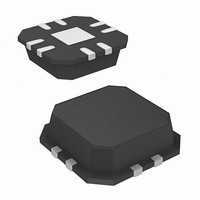
ISL6208ACRZ Intersil, ISL6208ACRZ Datasheet - Page 8

ISL6208ACRZ
Manufacturer Part Number
ISL6208ACRZ
Description
IC MOSFET DRVR SYNC BUCK 8-QFN
Manufacturer
Intersil
Datasheet
1.ISL6208ACBZ.pdf
(10 pages)
Specifications of ISL6208ACRZ
Configuration
High and Low Side, Synchronous
Input Type
PWM
Delay Time
26ns
Current - Peak
2A
Number Of Configurations
1
Number Of Outputs
2
High Side Voltage - Max (bootstrap)
33V
Voltage - Supply
4.5 V ~ 5.5 V
Operating Temperature
-10°C ~ 100°C
Mounting Type
Surface Mount
Package / Case
8-VQFN
Lead Free Status / RoHS Status
Lead free / RoHS Compliant
The equation can be rewritten to solve for R
follows:
Internal Bootstrap Diode
This driver features an internal bootstrap Schottky diode.
Simply adding an external capacitor across the BOOT and
PHASE pins completes the bootstrap circuit.
The bootstrap capacitor must have a maximum voltage rating
above the maximum battery voltage plus 5V. The bootstrap
capacitor can be chosen from the following equation:
where Q
charge the gate of the upper MOSFET. The ∆V
defined as the allowable droop in the rail of the upper drive.
As an example, suppose an upper MOSFET has a gate
charge, Q
the drive voltage over a PWM cycle is 200mV. One will find
that a bootstrap capacitance of at least 0.125µF is required.
The next larger standard value capacitance is 0.15µF. A
good quality ceramic capacitor is recommended.
Power Dissipation
Package power dissipation is mainly a function of the
switching frequency and total gate charge of the selected
MOSFETs. Calculating the power dissipation in the driver for
a desired application is critical to ensuring safe operation.
Exceeding the maximum allowable power dissipation level
will push the IC beyond the maximum recommended
operating junction temperature of 125°C. The maximum
allowable IC power dissipation for the SO-8 package is
approximately 800mW. When designing the driver into an
application, it is recommended that the following calculation
be performed to ensure safe operation at the desired
R
C
DELAY
BOOT
FIGURE 10. BOOTSTRAP CAPACITANCE vs BOOT RIPPLE
2.0
1.8
1.6
1.4
1.2
1.0
0.8
0.6
0.4
0.2
0.0
≥
(
0.0
GATE
kΩ
----------------------- -
∆V
GATE
Q
20nC
GATE
)
BOOT
0.1
=
VOLTAGE
is the amount of gate charge required to fully
, of 25nC at 5V and also assume the droop in
(
------------------------------------------------------
T
DELAY ns
0.2
Q
GATE
0.045
0.3
(
= 100nC
∆V
)
0.4
–
BOOT_CAP
5ns
8
0.5
)
0.6
(V)
0.7
DELAY
BOOT
0.8
as
0.9
term is
(EQ. 1)
1.0
ISL6208A
frequency for the selected MOSFETs. The power dissipated
by the driver is approximated as:
where f
and V
and Q
MOSFET selection and any external capacitance added to
the gate pins. The lV
of the driver and is typically negligible.
P
=
1000
f
900
800
700
600
500
400
300
200
100
sw
L
FIGURE 11. POWER DISSIPATION vs FREQUENCY
L
0
sw
represent the upper and lower gate rail voltage. Q
(
is the upper and lower gate charge determined by
0
1.5V
is the switching frequency of the PWM signal. V
Q
Q
200
U
U
L
=200nC
=100nC
Q
U
400
+
V
CC
L
600
Q
L
V
Q
)
Q
FREQUENCY (kHz)
CC
L
+
U
=100nC
800 1000 1200 1400 1600 1800 2000
I
=50nC
VCC
product is the quiescent power
V
CC
Q
Q
February 15, 2006
U
L
Q
Q
=50nC
=50nC
U
L
=50nC
=20nC
(EQ. 2)
FN9272.0
U
U


