IR21363JPBF International Rectifier, IR21363JPBF Datasheet - Page 4
IR21363JPBF
Manufacturer Part Number
IR21363JPBF
Description
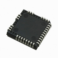
IC DRIVER 3-PHASE 44-PLCC
Manufacturer
International Rectifier
Specifications of IR21363JPBF
Configuration
3 Phase Bridge
Input Type
Inverting
Delay Time
425ns
Current - Peak
200mA
Number Of Configurations
1
Number Of Outputs
3
High Side Voltage - Max (bootstrap)
600V
Voltage - Supply
12 V ~ 20 V
Operating Temperature
-40°C ~ 125°C
Mounting Type
Surface Mount
Package / Case
44-PLCC (32 Leads)
Peak Output Current
350mA
Input Delay
525ns
Output Delay
500ns
Supply Voltage Range
12V To 20V
Driver Case Style
LCC
No. Of Pins
32
Operating Temperature Range
-40°C To +125°C
Rohs Compliant
Yes
Family Hvic
General Purpose HVICs
Channels
6
Topology
Three Phase
Application
General Purpose / Motor Control / PDP
Voffset
600
Io+ (ma)
200
Io- (ma)
350
Shutdown / Reset
Yes
Separate Power And Logic Ground
Yes
Over Current Protection
Yes
Uvlo
Vcc / Vbs
Vbsuv+ / Vccuv+ Min (v)
10.6
Vbsuv+ / Vccuv+ Typ (v)
11.1
Vbsuv+ / Vccuv+ Max (v)
11.6
Vbsuv- / Vccuv- Min (v)
10.4
Vbsuv- / Vccuv- Typ (v)
10.9
Dt / Sdt Min (ns)
220
Dt / Sdt Typ (ns)
290
Dt / Sdt Max (ns)
360
T On Min (ns)
300
T On Typ (ns)
425
T On Max (ns)
550
T Off Min (ns)
250
T Off Typ (ns)
400
T Off Max (ns)
550
Fault Reporting
Yes
Inverter Input Logic
LIN / HIN
Package
28 or 44 Lead
Part Status
Active & Preferred
Lead Free Status / RoHS Status
Lead free / RoHS Compliant
Available stocks
Company
Part Number
Manufacturer
Quantity
Price
Company:

Part Number:
IR21363JPBF
Manufacturer:
International Rectifier
Quantity:
10 000


Static Electrical Characteristics - (Continued)
V
applicable to all six channels (HIN1,2,3 and LIN1,2,3). The V
are applicable to the respective output leads: HO1,2,3 and LO1,2,3.
www.irf.com
BIAS
Symbol
R
V
(V
R
V
V
V
V
IN,CLAMP
on_FAULT
I
I
on_RCIN
I
I
ITRIP+
CCUVH
I
I
I
I
ITRIP-
CC
BSUVH
I
I
CCUV-
I
BSUV-
HIN+
RCIN
QBS
QCC
LIN+
I
I
HIN-
EN+
I
LIN-
EN-
O+
LK
O-
,V
BS1,2,3
) = 15 V unless otherwise specified. The V
V
undervoltage negative going
V
undervoltage lockout
Offset supply leakage current
Quiescent V
Quiescent V
Input clamp voltage (HIN, LIN, ITRIP and EN)
Input bias current (LOUT = HI)
Input bias current (LOUT = LO)
Input bias current (HOUT = HI)
Input bias current (HOUT = LO)
“High” ITRIP input bias current
“Low” ITRIP input bias current
“High” ENABLE input bias current
“Low” ENABLE input bias current
RCIN input bias current
Output high short circuit pulsed current
Output low short circuit pulsed current
RCIN low on resistance
FAULT low on resistance
threshold
hysteresis
CC
CC
and V
and V
BS
BS
BS
CC
supply
supply
supply current
supply current
Definition
IR213(6,62,63,65,66,67,68)(J&S) & PbF
IR2136(8)
IR21362
IR2136(3,5,6,7) 10.4 10.9
IR2136
IR21362
IR2136(3,5)
IR2136(2,3,5)
IR2136(6,7,8)
IR2136(2,3,5)
IR2136(6,7,8)
IR2136(3,5)
IR21362
IR2136(6,7,8)
IR2136(3,5)
IR2136(2,6,7,8) —
O
IN
and I
, V
TH
O
, and I
parameters are referenced to COM and V
Min Typ Max Units Test Conditions
120
250
7.4
8.6
0.3
0.5
4.9
—
—
—
—
—
—
—
—
—
—
—
—
—
—
—
—
—
—
—
IN
parameters are referenced to V
200
100
200
100
200
350
8.2
9.4
0.7
1.0
0.2
1.6
5.2
70
30
30
30
30
30
50
50
—
0
0
0
0
0
10.2
11.4
120
300
100
220
300
100
100
220
100
100
100
100
9.0
2.3
5.5
50
—
—
—
—
—
1
1
1
1
1
mA
mA
µA
µA
Ω
V
V
V
V
B1,2,3
V
Vrcin= 0 V or
IN
V
V
I
V
PW ≤10 µs
PW ≤10 µs
V
V
ENABLE
Vo =15 V,
IN
V
V
ENABLE
Vo =0 V,
= 0 V or 5 V
ITRIP
ITRIP
HIN
HIN
LIN
LIN
600 V
=100 µA
15 V
= V
= 5 V
= 0 V
= 5 V
= 0 V
SS
= 5 V
= 0 V
= 5 V
=0 V
S1,2,3
S1,2,3
and are
=
and
4
Related parts for IR21363JPBF
Image
Part Number
Description
Manufacturer
Datasheet
Request
R

Part Number:
Description:
IC DRIVER BRIDGE 3-PHASE 28-DIP
Manufacturer:
International Rectifier
Datasheet:

Part Number:
Description:
SCHOTTKY RECTIFIER
Manufacturer:
International Rectifier Corp.
Datasheet:
Part Number:
Description:
SCHOTTKY RECTIFIER
Manufacturer:
International Rectifier Corp.
Datasheet:
Part Number:
Description:
SCHOTTKY RECTIFIER
Manufacturer:
International Rectifier Corp.
Datasheet:
Part Number:
Description:
SCHOTTKY RECTIFIER
Manufacturer:
International Rectifier Corp.
Datasheet:
Part Number:
Description:
SCHOTTKY RECTIFIER
Manufacturer:
International Rectifier Corp.
Datasheet:
Part Number:
Description:
SCHOTTKY RECTIFIER
Manufacturer:
International Rectifier Corp.
Datasheet:
Part Number:
Description:
SCHOTTKY RECTIFIER
Manufacturer:
International Rectifier Corp.
Datasheet:
Part Number:
Description:
SCHOTTKY RECTIFIER
Manufacturer:
International Rectifier Corp.
Datasheet:
Part Number:
Description:
SCHOTTKY RECTIFIER
Manufacturer:
International Rectifier Corp.
Datasheet:
Part Number:
Description:
SCHOTTKY RECTIFIER
Manufacturer:
International Rectifier Corp.
Datasheet:
Part Number:
Description:
SCHOTTKY RECTIFIER
Manufacturer:
International Rectifier Corp.
Datasheet:
Part Number:
Description:
SCHOTTKY RECTIFIER
Manufacturer:
International Rectifier Corp.
Datasheet:
Part Number:
Description:
SCHOTTKY RECTIFIER
Manufacturer:
International Rectifier Corp.
Datasheet:
Part Number:
Description:
SCHOTTKY RECTIFIER
Manufacturer:
International Rectifier Corp.
Datasheet: