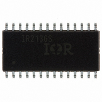
IR2136STRPBF International Rectifier, IR2136STRPBF Datasheet - Page 3

IR2136STRPBF
Manufacturer Part Number
IR2136STRPBF
Description
IC DRIVER BRIDGE 3PHASE 28SOIC
Manufacturer
International Rectifier
Datasheet
1.IR21362JTRPBF.pdf
(36 pages)
Specifications of IR2136STRPBF
Configuration
3 Phase Bridge
Input Type
Inverting
Delay Time
425ns
Current - Peak
200mA
Number Of Configurations
1
Number Of Outputs
3
High Side Voltage - Max (bootstrap)
600V
Voltage - Supply
10 V ~ 20 V
Operating Temperature
-40°C ~ 125°C
Mounting Type
Surface Mount
Package / Case
28-SOIC (7.5mm Width)
Number Of Drivers
6
Driver Configuration
Inverting
Driver Type
High and Low Side
Input Logic Level
CMOS/LSTTL/3.3V
Rise Time
190ns
Fall Time
75ns
Operating Supply Voltage (max)
20V
Peak Output Current
350uA
Power Dissipation
1.6W
Operating Supply Voltage (min)
10V
Turn Off Delay Time
550ns
Turn On Delay Time (max)
550ns
Operating Temp Range
-40C to 125C
Operating Temperature Classification
Automotive
Mounting
Surface Mount
Pin Count
28
Package Type
SOIC W
Lead Free Status / RoHS Status
Lead free / RoHS Compliant
Other names
IR2136SPBFTR
IR2136STRPBF
IR2136STRPBFTR
IR2136STRPBF
IR2136STRPBFTR
Available stocks
Company
Part Number
Manufacturer
Quantity
Price
Company:
Part Number:
IR2136STRPBF
Manufacturer:
RENESAS
Quantity:
3 000
Part Number:
IR2136STRPBF
Manufacturer:
IR
Quantity:
20 000
Recommended Operating Conditions - (Continued)
The input/output logic-timing diagram is shown in Fig. 1. For proper operation the device should be used within the
recommended conditions. All voltage parameters are absolute referenced to COM. The V
with all supplies biased at a 15 V differential.
Note 2: All input pins and the ITRIP and EN pins are internally clamped with a 5.2 V zener diode.
Static Electrical Characteristics
V
applicable to all six channels (HIN1,2,3 and LIN1,2,3). The V
and are applicable to the respective output leads: HO1,2,3 and LO1,2,3.
www.irf.com
BIAS
Symbol
V
(V
V
Symbol
V
V
V
V
V
V
RCIN, TH+
RCIN, HYS
V
CC
EN,TH+
EN,TH-
V
V
CCUV+
V
IT,HYS
BSUV+
V
IT,TH+
V
ITRIP
T
OH
OL
IN
,V
A
IH
IL
BS1,2,3
) = 15 V unless otherwise specified. The V
Logic “0” input voltage LIN1,2,3, HIN1,2,3
IR213(6,63,65)
Logic “1” input voltage HIN1,2,3 IR21362
Logic “0” input voltage LIN1,2,3, HIN1,2,3
IR213(66,67,68)
Logic “1” input Voltage LIN1,2,3, HIN1,2,3
IR213(6,63,65)
Logic “0” input voltage HIN1,2,3 IR21362
Logic “0” input voltage LIN1,2,3, HIN1,2,3
IR213(66,67,68)
Enable positive going threshold
Enable negative going threshold
ITRIP positive going
threshold
ITRIP input hysteresis
RCIN positive going threshold
RCIN input hysteresis
High level output voltage, V
Low level output voltage, V
V
undervoltage positive going
threshold
ITRIP input voltage
Logic input voltage LIN, HIN (IR213(6,63,65,66,67,68)),
HIN (IR21362), EN
Ambient temperature
CC
and V
BS
supply
Definition
IR213(6,62,63,65,66,67,68)(J&S) & PbF
Definition
O
BIAS
IR2136(2)(3)(6)
IR21365(7)(8)
IR2136(2)(3)(6)
IR21365(7)(8)
IR2136(8)
IR21362
IR21363(5)(6)(7) 10.6 11.1
- V
O
IN
O
, V
and I
TH
, and I
O
parameters are referenced to COM and V
IN
0.37 0.46
3.85 4.30
Min
3.0
2.5
0.8
8.0
9.6
—
—
—
—
—
—
—
—
parameters are referenced to V
0.07
10.4
Typ
.15
0.9
0.4
8.9
—
—
—
—
—
8
3
Max Units Test Conditions
0.55
4.75
11.2
11.6
0.8
1.4
0.6
9.8
—
—
—
—
—
—
—
3
S
Min
offset ratings are tested
V
V
-40
SS
SS
V
V
V
Max
Io = 20 mA
SS
SS
125
+ 5
+ 5
SS
and are
Units
S1,2,3
°C
V
3


