IXDF502SIAT/R IXYS, IXDF502SIAT/R Datasheet
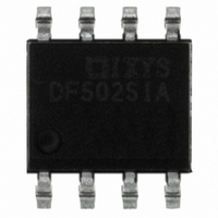
IC MOSF DRIVER FAST DUAL 8-SOIC

IXDF502SIAT/R

Manufacturer Part Number
IXDF502SIAT/R
Description
IC MOSF DRIVER FAST DUAL 8-SOIC
Manufacturer
IXYS
Type
Low Sider
Datasheet

Specifications of IXDF502SIAT/R

Configuration
Low-Side
Input Type
Inverting and Non-Inverting
Delay Time
25ns
Current - Peak
2A
Number Of Configurations
2
Number Of Outputs
2
Voltage - Supply
4.5 V ~ 30 V
Operating Temperature
-55°C ~ 125°C
Mounting Type
Surface Mount
Package / Case
8-SOIC
Rise Time
10 ns
Fall Time
9 ns
Supply Voltage (min)
4.5 V
Supply Current
3 mA
Maximum Operating Temperature
+ 125 C
Mounting Style
SMD/SMT
Minimum Operating Temperature
- 55 C
Number Of Drivers
2
Lead Free Status / RoHS Status
Lead free / RoHS Compliant
High Side Voltage - Max (bootstrap)
-
Lead Free Status / Rohs Status
Lead free / RoHS Compliant
Other names
IXDF502SIATR
Features
• Built using the advantages and compatibility
• Latch-Up Protected up to 2 Amps
• High 2A Peak Output Current
• Wide Operating Range: 4.5V to 30V
• -55°C to +125°C Extended Operating
• High Capacitive Load
• Matched Rise And Fall Times
• Low Propagation Delay Time
• Low Output Impedance
• Low Supply Current
• Two Drivers in Single Chip
Applications
• Driving MOSFETs and IGBTs
• Motor Controls
• Line Drivers
• Pulse Generators
• Local Power ON/OFF Switch
• Switch Mode Power Supplies (SMPS)
• DC to DC Converters
• Pulse Transformer Driver
• Class D Switching Amplifiers
• Power Charge Pumps
Copyright © 2007 IXYS CORPORATION All rights reserved
of CMOS and IXYS HDMOS
Temperature
Drive Capability: 1000pF in <10ns
Ordering Information
NOTE: All parts are lead-free and RoHS Compliant
Part Number
IXDF502PI
IXDF502SIA
IXDF502SIAT/R 2A Low Side Gate Driver I.C.
IXDF502D1
IXDF502D1T/R
IXDI502PI
IXDI502SIA
IXDI502SIAT/R
IXDI502D1
IXDI502D1T/R
IXDN502PI
IXDN502SIA
IXDN502SIAT/R 2A Low Side Gate Driver I.C.
IXDN502D1
IXDN502D1T/R
2 Ampere Dual Low-Side Ultrafast MOSFET Drivers
Description
2A Low Side Gate Driver I.C.
IXDF502 / IXDI502 / IXDN502
TM
processes
Package
Type
8-Pin PDIP
8-Pin SOIC
8-Pin SOIC
6-Lead DFN
6-Lead DFN
8-Pin PDIP
8-Pin SOIC
8-Pin SOIC
6-Lead DFN
6-Lead DFN
8-Pin PDIP
8-Pin SOIC
8-Pin SOIC
6-Lead DFN
6-Lead DFN
General Description
The IXDF502, IXDI502 and IXDN502 each consist of two 2-
Amp CMOS high speed MOSFET Gate Drivers for driving
the latest IXYS MOSFETs & IGBTs. Each of the Dual
Outputs can source and sink 2 Amps of Peak Current while
producing voltage rise and fall times of less than 15ns. The
input of each Driver is TTL or CMOS compatible and is
virtually immune to latch up. Patented* design innovations
eliminate cross conduction and current "shoot-through".
Improved speed and drive capabilities are further enhanced
by very quick & matched rise and fall times.
The IXDF502 is configured with one Gate Driver Inverting
plus one Gate Driver Non-Inverting. The IXDI502 is config-
ured as a Dual Inverting Gate Driver, and the IXDN502 is
configured as a Dual Non-Inverting Gate Driver.
The IXDF502, IXDI502 and IXDN502 are each available in
the 8-Pin P-DIP (PI) package, the 8-Pin SOIC (SIA) pack-
age, and the 6-Lead DFN (D1) package, (which occupies
less than 65% of the board area of the 8-Pin SOIC).
*United States Patent 6,917,227
Packing Style
Tube
Tube
13” Tape and Reel
2” x 2” Waffle Pack
13” Tape and Reel
Tube
Tube
13” Tape and Reel
2” x 2” Waffle Pack
13” Tape and Reel
Tube
Tube
13” Tape and Reel
2” x 2” Waffle Pack
13” Tape and Reel
First Release
Pack
Qty
2500
2500
2500
2500
2500
2500
50
94
56
50
94
56
50
94
56
Configuration
Driver Inverting
and one Driver
Dual, with both
Dual, with both
Dual, with one
Non-Inverting
Drivers Non-
Inverting
Inverting
Drivers
DS99573B(03/10)

Related parts for IXDF502SIAT/R

IXDF502SIAT/R Summary of contents

Page 1

... Ordering Information Part Number Description IXDF502PI 2A Low Side Gate Driver I.C. IXDF502SIA 2A Low Side Gate Driver I.C. IXDF502SIAT/R 2A Low Side Gate Driver I.C. IXDF502D1 2A Low Side Gate Driver I.C. IXDF502D1T/R 2A Low Side Gate Driver I.C. IXDI502PI 2A Low Side Gate Driver I.C. ...

Page 2

... GND Figure 2 - IXDI502 Dual Inverting 2A Gate Driver Functional Block Diagram GND Figure 3 - IXDN502 Dual 2A Non-Inverting Gate Driver Functional Block Diagram GND * United States Patent 6,917,227 Copyright © 2007 IXYS CORPORATION All rights reserved IXDF502 / IXDI502 / IXDN502 Vcc P ANTI-CROSS OUT A CONDUCTION * CIRCUIT * N P ...

Page 3

... On-time propagation delay ONDLY t Off-time propagation delay OFFDLY V Power supply voltage CC I Power supply current CC IXYS reserves the right to change limits, test conditions, and dimensions. IXDF502 / IXDI502 / IXDN502 (1) Operating Ratings Parameter Operating Supply Voltage + 0.3V Operating Temperature Range CC Package Thermal Resistance * 8-Pin PDIP ...

Page 4

... U.S. or Europe, and not a premium Japanese IMS mil dialectric with a thermal conductivity of 2.2W/mC was assumed. The result was given as typical, and indicates what a user would expect on a typical IMS substrate, and shows the potential low thermal resistance for the DFN package. Copyright © 2007 IXYS CORPORATION All rights reserved IXDF502 / IXDI502 / IXDN502 o ...

Page 5

... NOTE: Solder tabs on bottoms of DFN packages are grounded Figure 4 - Characteristics Test Diagram Vcc 10uF IXYS reserves the right to change limits, test conditions, and dimensions. IXDF502 / IXDI502 / IXDN502 FUNCTION A Channel Input A Channel Input signal-TTL or CMOS compatible. The system ground pin. Internally connected to all circuitry, this pin provides ground reference for the entire chip ...

Page 6

... Fall time - Temperature (C) Fall Time vs. Capacitive Load Fig 100 1000 Load Capacitance (pF) Copyright © 2007 IXYS CORPORATION All rights reserved IXDF502 / IXDI502 / IXDN502 Typical Performance Characteristics Fig. 6 10000pF 5400pF 1000pF 560pF Fig 1000pF 100 150 Fig 10V 15V 20V 10000 6 Fall Time vs. Supply Voltage ...

Page 7

Fig. 11 Input Threshold Levels vs. Temperature 3 2.5 2 Positive going input 1.5 Negative going input 1 0 Temperature (C) Fig. 13 Propagation Delay vs. Supply Voltage Falling Input, C LOAD ...

Page 8

... Load Capacitance (pF) Fig. 21 Supply Current vs. Capacitive Load V = 15V SUPPLY 300 250 200 150 100 50 0 100 1000 Load Capacitance (pF) Copyright © 2007 IXYS CORPORATION All rights reserved IXDF502 / IXDI502 / IXDN502 Fig. 18 Supply Current vs. Frequency 100 2MHz 1MHz 100kHz 0 10000 100 Supply Current vs ...

Page 9

Fig. 23 Supply Current vs. Capacitive Load V = 20V SUPPLY 400 350 300 250 200 150 100 50 0 100 1000 Load Capacitance (pF) Fig. 25 Output Source Current vs. Supply Voltage ...

Page 10

... Fig. 29 High State Output Resistance vs. Supply Voltage Supply Voltage (V) Copyright © 2007 IXYS CORPORATION All rights reserved IXDF502 / IXDI502 / IXDN502 Fig. 30 Low State Output Resistance vs. Supply Voltage 4.5 4 3.5 3 2.5 2 1 Supply Voltage ( ...

Page 11

Supply Bypassing, Grounding Practices And Output Lead inductance When designing a circuit to drive a high speed MOSFET utilizing the IXD_502 very important to observe certain design criteria in order to optimize performance of the driver. Particular attention ...

Page 12

... 0.035 [0.90] 0.197± 0.005 [5.00± 0.13 S0.002^ 0.000; o S0.05^ 0.00;o Copyright © 2007 IXYS CORPORATION All rights reserved IXDF502 / IXDI502 / IXDN502 0.137 [3.48] IXYS Corporation 3540 Bassett St; Santa Clara, CA 95054 Tel: 408-982-0700; Fax: 408-496-0670 e-mail: sales@ixys.net www.ixys.com 0.018 [0.47] ...

Related keywords