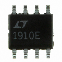
LT1910ES8#TR Linear Technology, LT1910ES8#TR Datasheet - Page 9

LT1910ES8#TR
Manufacturer Part Number
LT1910ES8#TR
Description
IC DRIVER MOSFET HI SIDE 8SOIC
Manufacturer
Linear Technology
Datasheet
1.LT1910ES8PBF.pdf
(12 pages)
Specifications of LT1910ES8#TR
Configuration
High-Side
Input Type
Non-Inverting
Delay Time
220µs
Number Of Configurations
1
Number Of Outputs
1
Voltage - Supply
8 V ~ 48 V
Operating Temperature
-40°C ~ 85°C
Mounting Type
Surface Mount
Package / Case
8-SOIC (3.9mm Width)
Lead Free Status / RoHS Status
Contains lead / RoHS non-compliant
Current - Peak
-
High Side Voltage - Max (bootstrap)
-
Available stocks
Company
Part Number
Manufacturer
Quantity
Price
APPLICATIONS INFORMATION
The turn-on current spike into C
where V
obtained by plotting the equation:
on the graph of Gate Drive Current (I
(V
intersection of the curves for a given supply is V
example, if V
V
I
network ensure fast current limit turn-off.
When turning off a capacitive load, the source of the
MOSFET can “hang up” if the load resistance does not
discharge C
If this is the case, a 15V zener may be added from gate to
source to prevent V
Adding Current Limit Delay
When capacitive loads are being switched or in very noisy
environments, it is desirable to add delay in the drain
current-sense path to prevent false tripping (inductive
loads normally do not need delay). This is accomplished
by the current limit delay network shown in Figure 5.
PEAK
TH
GATE
I
I
PEAK
GATE
= 2V, C1 = 0.1μF and C
= 1.6A. The diode and the second resistor in the
) as shown in Figure 6. The value of V
TH
=
=
Figure 6. Gate Drive Current vs Gate Voltage
400
200
800
700
600
500
300
100
C
V
is the MOSFET gate threshold voltage. V
LOAD
LOAD
0
GATE
R
+
0
1
= 24V and R1 = 100k, then V
V
as fast as the gate is being pulled down.
•
+
10
= 24V
V
V
GS(MAX)
+
R C
G
V
= 12V
• 1 1
+
–
GATE VOLTAGE (V)
20
= 8V
V
TH
LOAD
30
from being exceeded.
V
+
= 48V
LOAD
= 1000μF , the estimated
40
GATE
I
V
GATE
GATE
is estimated by:
50
) vs Gate Voltage
=
/10
1910 F06
5
60
G
= 18.3V. For
GATE
G
at the
. For
G
is
R
to approximately 10 • I
and provides immediate turn-off (see Figure 7). To ensure
proper operation of the timer, C
Printed Circuit Board Shunts
The sheet resistance of 1oz copper clad is approximately
5 • 10
0.39%/°C. Since the LT1910 drain-sense threshold has a
similar temperature coeffi cient (0.33%/°C), this offers the
possibility of nearly zero TC current sensing using the “free”
drain-sense resistor made out of PC trace material.
A conservative approach is to use 0.02" of width for each
1A of current for 1oz copper. Combining the LT1910 drain
sense threshold with the 1oz copper resistance results in
a simple expression for width and length:
The width for 2oz copper would be halved while the length
would remain the same.
Bends may be incorporated into the resistor to reduce
space; each bend is equivalent to approximately 0.6 •
the width of a straight length. Kelvin connection should
be employed by running a separate trace from the ends
of the resistor back to the LT1910’s V
See Application Note 53 for further information on printed
circuit board shunts.
D
Width (1oz Cu) = 0.02" • I
Length (1oz Cu) = 2"
and C
–4
D
Ω/square with a temperature coeffi cient of
0.01
delay the overcurrent trip for drain currents up
0.1
10
1
Figure 7. Current Limit Delay Time
1
MOSFET DRAIN CURRENT (1 = SET CURRENT)
SET
, above which the diode conducts
10
SET
D
must be ≤C
+
and SENSE pins.
1910 F07
100
LT1910
T
.
1910fa
9


