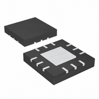
MAX5064BATC+ Maxim Integrated Products, MAX5064BATC+ Datasheet - Page 9

MAX5064BATC+
Manufacturer Part Number
MAX5064BATC+
Description
IC MOSFET DRIVER 12-TQFN
Manufacturer
Maxim Integrated Products
Type
High Side/Low Sider
Datasheet
1.MAX5063AASA.pdf
(20 pages)
Specifications of MAX5064BATC+
Configuration
Half Bridge
Input Type
Differential
Delay Time
35ns
Current - Peak
2A
Number Of Configurations
1
Number Of Outputs
2
High Side Voltage - Max (bootstrap)
125V
Voltage - Supply
8 V ~ 12.6 V
Operating Temperature
-40°C ~ 125°C
Mounting Type
Surface Mount
Package / Case
12-TQFN Exposed Pad
Rise Time
65 ns
Fall Time
65 ns
Supply Voltage (min)
8 V
Supply Current
3 mA
Maximum Power Dissipation
1951.2 mW
Maximum Operating Temperature
+ 125 C
Mounting Style
SMD/SMT
Bridge Type
Half Bridge
Minimum Operating Temperature
- 40 C
Number Of Drivers
2
Lead Free Status / RoHS Status
Lead free / RoHS Compliant
Figure 1. Timing Characteristics for Noninverting and Inverting Logic Inputs
The MAX5062/MAX5063/MAX5064 are 125V/2A high-
speed, half-bridge MOSFET drivers that operate from a
supply voltage of +8V to +12.6V. The drivers are
intended to drive a high-side switch without any isola-
tion device like an optocoupler or drive transformer.
The high-side driver is controlled by a TTL/CMOS logic
signal referenced to ground. The 2A source and sink
drive capability is achieved by using low R
and n-channel driver output stages. The BiCMOS
process allows extremely fast rise/fall times and low
IN_H+
IN_L+
IN_H-
IN_L-
_______________________________________________________________________________________
t
t
DH
MATCH1
MATCH2
DL
Detailed Description
= (t
= (t
V
V
V
V
IH
IL
IH
D_ON2
D_ON3
IL
- t
- t
D_ON1
D_ON1
) or (t
) or (t
t
D_OFF3
t
t
t
D_OFF4
D_OFF1
D_OFF2
D_OFF2
D_ON4
- t
- t
D_ON2
D_OFF1
DS_ON
) or (t
)
Half-Bridge MOSFET Drivers
D_OFF3
p-
- t
t
t
D_OFF1
F
F
V
V
) or (t
IL
IL
propagation delays. The typical propagation delay from
the logic-input signal to the drive output is 35ns with a
matched propagation delay of 3ns typical. Matching
these propagation delays is as important as the
absolute value of the delay itself. The high 125V input
voltage range allows plenty of margin above the 100V
transient specification per telecom standards.
The MAX5064 is available in a thermally enhanced
TQFN package, which can dissipate up to 1.95W (at
+70°C) and allow up to 1MHz switching frequency
while driving 100nC combined gate-charge MOSFETs.
D_OFF4
125V/2A, High-Speed,
V
V
- t
IH
IH
D_OFF2
)
t
t
t
D_ON4
D_ON1
t
D_ON3
D_ON2
90%
10%
t
90%
10%
t
R
R
9


