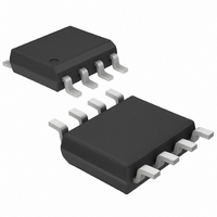
MAX5055BASA+ Maxim Integrated Products, MAX5055BASA+ Datasheet - Page 14

MAX5055BASA+
Manufacturer Part Number
MAX5055BASA+
Description
IC MOSFET DRVR DUAL 8-SOIC
Manufacturer
Maxim Integrated Products
Type
Low Sider
Datasheet
1.MAX5054AATAT.pdf
(15 pages)
Specifications of MAX5055BASA+
Configuration
Low-Side
Input Type
Inverting
Delay Time
20ns
Current - Peak
4A
Number Of Configurations
2
Number Of Outputs
2
Voltage - Supply
4 V ~ 15 V
Operating Temperature
-40°C ~ 125°C
Mounting Type
Surface Mount
Package / Case
8-SOIC (3.9mm Width)
Rise Time
85 ns
Fall Time
75 ns
Supply Voltage (min)
4 V
Supply Current
2.4 mA
Maximum Power Dissipation
471 mW
Maximum Operating Temperature
+ 125 C
Mounting Style
SMD/SMT
Maximum Turn-off Delay Time
35 ns
Maximum Turn-on Delay Time
35 ns
Minimum Operating Temperature
- 40 C
Number Of Drivers
2
Lead Free Status / RoHS Status
Lead free / RoHS Compliant
High Side Voltage - Max (bootstrap)
-
Lead Free Status / Rohs Status
Lead free / RoHS Compliant
4A, 20ns, Dual MOSFET Drivers
* EP = Exposed pad.
14
MAX5054AATA
MAX5054BATA
MAX5055AASA
MAX5055BASA
MAX5056AASA
MAX5056BASA
MAX5057AASA
MAX5057BASA
______________________________________________________________________________________
PART
TOP VIEW
PIN-
PACKAGE
8 TDFN-EP*
8 TDFN-EP*
8 SO-EP*
8 SO
8 SO-EP*
8 SO
8 SO-EP*
8 SO
OUTB
INA+
INB+
INA-
INB-
GND
GND
N.C.
V
and Dual Noninverting Inputs
TTL Dual Inverting and Dual
Noninverting Inputs
TTL Dual Inverting Inputs
TTL Dual Inverting Inputs
TTL Dual Noninverting Inputs
TTL Dual Noninverting Inputs
TTL Inverting and
Noninverting Inputs
TTL Inverting and
Noninverting Inputs
DD
1
2
4
1
2
4
3
3
Selector Guide
/ 2 CMOS Dual Inverting
SO/SO-EP
TDFN-EP
LOGIC INPUT
MAX5054
MAX5056
8
7
6
5
8
7
6
5
INA+
INB+
OUTA
V
N.C.
OUTA
V
OUTB
DD
DD
For the latest package outline information and land patterns, go
to www.maxim-ic.com/packages. Note that a “+”, “#”, or “-” in
the package code indicates RoHS status only. Package draw-
ings may show a different suffix character, but the drawing per-
tains to the package regardless of RoHS status.
PROCESS: CMOS
PACKAGE
8 TDFN-EP
INB+
INA-
GND
INB-
INA-
GND
N.C.
N.C.
8 SO-EP
TYPE
8 SO
1
2
4
1
2
4
3
3
SO/SO-EP
SO/SO-EP
MAX5055
MAX5057
PACKAGE
S8E+14
T833+2
CODE
S8+4
Package Information
6
6
8
7
5
8
7
5
Pin Configurations
N.C.
V
N.C.
V
OUTA
OUTB
OUTA
OUTB
DD
DD
OUTLINE NO.
Chip Information
21-0137
21-0111
21-0041
PATTERN NO.
90-0059
90-0151
90-0096
LAND


