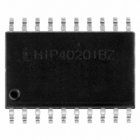
HIP4020IBZ Intersil, HIP4020IBZ Datasheet - Page 4

HIP4020IBZ
Manufacturer Part Number
HIP4020IBZ
Description
IC DRIVER FULL-BRIDGE 20-SOIC
Manufacturer
Intersil
Datasheet
1.HIP4020IBZ.pdf
(9 pages)
Specifications of HIP4020IBZ
Configuration
H Bridge
Input Type
Inverting and Non-Inverting
Delay Time
2.5µs
Current - Peak
625mA
Number Of Configurations
1
Number Of Outputs
4
Voltage - Supply
3 V ~ 12 V
Operating Temperature
-40°C ~ 85°C
Mounting Type
Surface Mount
Package / Case
20-SOIC (7.5mm Width)
Lead Free Status / RoHS Status
Lead free / RoHS Compliant
High Side Voltage - Max (bootstrap)
-
Available stocks
Company
Part Number
Manufacturer
Quantity
Price
Part Number:
HIP4020IBZ
Manufacturer:
HARRIS
Quantity:
20 000
Company:
Part Number:
HIP4020IBZT
Manufacturer:
Intersil
Quantity:
2 000
Electrical Specifications
Pin Descriptions
Thermal Shutdown
Response Time: V
Turn-On: Prop Delay
Rise Time
Turn-Off: Prop Delay
Fall Time
PIN NUMBER
12, 19
14, 17
8, 5
9, 3
7, 4
15
16
6
2
PARAMETER
EN
to V
OUTA, OUTB
ENA, ENB
SYMBOL
OUT
A1, B1
A2, B2
V
V
V
V
ILF
SSA
SSB
DD
SS
4
T
A
= 25°C, V
Positive Power Supply pins; internally common and externally connect to the same Positive Supply (V+).
Negative Power Supply pin; Negative or Ground return for Switch Driver A; externally connect to the Supply
(V-).
Negative Power Supply pin; Negative or Ground return for Switch Driver B; externally connect to the Supply
(V-).
Common Ground pin for the Input Logic Control circuits. May be used as a common ground with V SSA and
V
Input pins used to control the direction of output load current to/from OUTA and OUTB, respectively. When
connected, A1 and B1 can be controlled from the same logic signal to change the directional rotation of a
motor.
Input pins used to force a low state on OUTA and OUTB, respectively. When connected, A2 and B2 can be
controlled from the same logic signal to activate Dynamic Braking of a motor.
Input pins used to Enable Switch Driver A and Switch Driver B, respectively. When Low, the respective
output is in a high impedance (Z) off-state. Since each Switch Driver is independently controlled, OUTA and
OUTB may be a separately PWM controlled as Half H-Switch Drivers.
Respectively, Switch Driver A and Switch Driver B Output pins.
Current Limiting Fault Output Flag pin; when in a high logic state, signifies that Switch Driver A or B or both
are in a Current Limiting Fault Mode.
SSB.
SYMBOL
DD
t
t
T
PLH
PHL
SD
t
t
r
f
= +5V, V
I
O
SSA
= 0.5A (Note 3)
HIP4020
= V
SSB
TEST CONDITIONS
= V
SS
= 0V, Unless Otherwise Specified (Continued)
DESCRIPTION
MIN
-
-
-
-
-
TYP
145
2.5
0.1
0.1
4
MAX
-
-
-
-
-
December 20, 2005
UNITS
FN3976.3
°C
µs
µs
µs
µs


