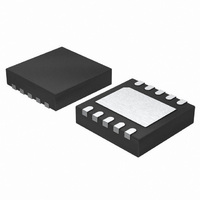
ISL6622CRZ-T Intersil, ISL6622CRZ-T Datasheet - Page 8

ISL6622CRZ-T
Manufacturer Part Number
ISL6622CRZ-T
Description
IC MOSFET DVR SYNC BUCK 10-DFN
Manufacturer
Intersil
Datasheet
1.ISL6622CRZ-T.pdf
(12 pages)
Specifications of ISL6622CRZ-T
Configuration
High and Low Side, Synchronous
Input Type
PWM
Delay Time
20ns
Current - Peak
1.25A
Number Of Configurations
1
Number Of Outputs
2
High Side Voltage - Max (bootstrap)
36V
Voltage - Supply
6.8 V ~ 13.2 V
Operating Temperature
0°C ~ 70°C
Mounting Type
Surface Mount
Package / Case
10-DFN
Lead Free Status / RoHS Status
Lead free / RoHS Compliant
Other names
ISL6622CRZ-T
Available stocks
Company
Part Number
Manufacturer
Quantity
Price
Company:
Part Number:
ISL6622CRZ-T
Manufacturer:
ST
Quantity:
581
Part Number:
ISL6622CRZ-T
Manufacturer:
INTERSIL
Quantity:
20 000
Part Number:
ISL6622CRZ-TS2378
Manufacturer:
INTERSIL
Quantity:
20 000
Pre-POR Overvoltage Protection
While VCC is below its POR level, the upper gate is held low
and LGATE is connected to the PHASE pin via an internal
10kΩ (typically) resistor. By connecting the PHASE node to
the gate of the low side MOSFET, the driver offers some
passive protection to the load if the upper MOSFET(s) is or
becomes shorted. If the PHASE node goes higher than the
gate threshold of the lower MOSFET, it results in the
progressive turn-on of the device and the effective clamping
of the PHASE node’s rise. The actual PHASE node clamping
level depends on the lower MOSFET’s electrical
characteristics, as well as the characteristics of the input
supply and the path connecting it to the respective PHASE
node.
Internal Bootstrap Device
The ISL6622 features an internal bootstrap Schottky diode.
Simply adding an external capacitor across the BOOT and
PHASE pins completes the bootstrap circuit. The bootstrap
function is also designed to prevent the bootstrap capacitor
from overcharging due to the large negative swing at the
trailing-edge of the PHASE node. This reduces the voltage
stress on the BOOT to PHASE pins.
The bootstrap capacitor must have a maximum voltage
rating well above the maximum voltage intended for UVCC.
Its minimum capacitance value can be estimated from
Equation 1:
where Q
at V
control MOSFETs. The ΔV
allowable droop in the rail of the upper gate drive. Select
results are exemplified in Figure 5.
C
Q
BOOT_CAP
UGATE
GS1
G1
gate-source voltage and N
=
Q
----------------------------------- - N
is the amount of gate charge per upper MOSFET
≥
G1
------------------------------------- -
ΔV
V
•
GS1
Q
BOOT_CAP
UVCC
UGATE
•
BOOT_CAP
Q1
8
Q1
term is defined as the
is the number of
(EQ. 1)
ISL6622
.
Power Dissipation
Package power dissipation is mainly a function of the
switching frequency (F
layout resistance, and the selected MOSFET’s internal gate
resistance and total gate charge (Q
dissipation in the driver for a desired application is critical to
ensure safe operation. Exceeding the maximum allowable
power dissipation level may push the IC beyond the maximum
recommended operating junction temperature. The DFN
package is more suitable for high frequency applications. See
“Layout Considerations” on page 9 for thermal impedance
improvement suggestions. The total gate drive power losses
due to the gate charge of MOSFETs and the driver’s internal
circuitry and their corresponding average driver current can
be estimated using Equations 2 and 3, respectively:
where the gate charge (Q
particular gate to source voltage (V
corresponding MOSFET datasheet; I
quiescent current with no load at both drive outputs; N
and N
respectively; UVCC and LVCC are the drive voltages for
both upper and lower FETs, respectively. The I
product is the quiescent power of the driver without a load.
P
I
DR
Qg_TOT
FIGURE 5. BOOTSTRAP CAPACITANCE vs BOOT RIPPLE
P
P
=
Qg_Q2
Qg_Q1
Q2
1.6
1.4
1.2
1.0
0.8
0.6
0.4
0.2
0.0
⎛
⎜
⎝
Q
----------------------------------------------------- -
0.0
are number of upper and lower MOSFETs,
G1
=
20nC
P
=
=
•
Qg_Q1
0.1
VOLTAGE
UVCC N
V
Q
-------------------------------------- - F
Q
------------------------------------- - F
GS1
G1
G2
0.2
V
V
•
•
+
50nC
Q
GS2
GS1
•
LVCC
UVCC
P
UGATE
SW
Qg_Q2
0.3
Q1
), the output drive impedance, the
G1
+
2
= 100nC
2
ΔV
0.4
•
Q
---------------------------------------------------- -
and Q
•
+
BOOT_CAP
G2
I
SW
Q
SW
0.5
•
•
G
LVCC N
•
VCC
V
G2
GS1
•
). Calculating the power
N
GS2
N
Q
Q2
) is defined at a
0.6
Q1
is the driver’s total
(V)
and V
•
0.7
Q2
GS2
⎞
⎟
⎠
Q*
0.8
•
October 30, 2008
VCC
F
) in the
SW
0.9
FN6470.2
(EQ. 2)
(EQ. 3)
Q1
+
I
Q
1.0


