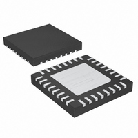
MAX16831ATJ+T Maxim Integrated Products, MAX16831ATJ+T Datasheet - Page 15

MAX16831ATJ+T
Manufacturer Part Number
MAX16831ATJ+T
Description
IC LED DRIVR HIGH BRIGHT 32-TQFN
Manufacturer
Maxim Integrated Products
Type
HBLED Driverr
Datasheet
1.MAX16831ATJT.pdf
(19 pages)
Specifications of MAX16831ATJ+T
Topology
PWM, Step-Down (Buck), Step-Up (Boost)
Number Of Outputs
1
Internal Driver
No
Type - Primary
Automotive
Type - Secondary
High Brightness LED (HBLED), RGB
Frequency
125kHz ~ 600kHz
Voltage - Supply
5.5 V ~ 76 V
Mounting Type
Surface Mount
Package / Case
32-TQFN Exposed Pad
Operating Temperature
-40°C ~ 125°C
Internal Switch(s)
Yes
Efficiency
90%
Lead Free Status / RoHS Status
Lead free / RoHS Compliant
Voltage - Output
-
Current - Output / Channel
-
Lead Free Status / Rohs Status
Details
When using the MAX16831 in a boost or buck-boost
configuration, the input RMS current is low and the
input capacitance can be small.
The MAX16831 can also be used in the absence of the
dimming MOSFET. In this case, the PWM dimming per-
formance is compromised but in applications that do
not require dimming, the MAX16831 can still be used.
A short circuit across the load will cause the MAX16831
to disable the gate drivers and they will remain off until
the input power is recycled.
When selecting MOSFETs for switching, consider the
total gate charge, power dissipation, the maximum
drain-to-source voltage, and package thermal imped-
ance. The product of the MOSFET gate charge and
R
fying better performance. Select MOSFETs optimized
for high-frequency switching applications.
MOSFET losses may be broken into three categories:
conduction loss, gate drive loss, and switching loss.
The following simplified power loss equation is true for
all the different configurations.
Typically, there are two sources of noise emission in a
switching power supply: high di/dt loops and high dv/dt
surfaces. For example, traces that carry the drain cur-
rent often form high di/dt loops. Similarly, the heatsink
of the MOSFET connected to the device drain presents
a high dv/dt source; therefore, minimize the surface
area of the heatsink as much as possible. Keep all PCB
traces carrying switching currents as short as possible
to minimize current loops. Use ground planes for best
results.
Careful PCB layout is critical to achieve low switching
losses and clean, stable operation. Use a multilayer
board whenever possible for better noise performance
and power dissipation. Follow these guidelines for
good PCB layout:
• Use a large copper plane under the MAX16831
DS(ON)
P
package. Ensure that all heat-dissipating compo-
nents have adequate cooling. Connect the exposed
pad of the device to the ground plane.
LOSS
Operating the MAX16831 Without the
is a figure of merit, with a lower number signi-
= P
Switching Power MOSFET Losses
CONDUCTION
High-Voltage, High-Power LED Driver with
______________________________________________________________________________________
Layout Recommendations
+ P
GATEDRIVE
Analog and PWM Dimming Control
Dimming Switch
+ P
SWITCH
• Isolate the power components and high-current paths
• Keep the high-current paths short, especially at the
• Connect AGND, SGND, and QGND to a ground
• Keep the power traces and load connections short.
• Ensure that the feedback connection to FB is short
• Route high-speed switching nodes away from the
• To prevent discharge of the compensation capaci-
from sensitive analog circuitry.
ground terminals. This practice is essential for sta-
ble, jitter-free operation. Keep switching loops short.
plane. Ensure a low-impedance connection between
all ground points.
This practice is essential for high efficiency. Use
thick copper PCBs (2oz vs. 1oz) to enhance full-load
efficiency.
and direct.
sensitive analog areas.
tors, C1 and C2, during the off-time of the dimming
cycle, ensure that the PCB area close to these com-
ponents has extremely low leakage. Discharge of
these capacitors due to leakage may result in
degraded dimming performance.
TOP VIEW
*EP = EXPOSED PAD
CLKOUT
RTSYNC
AGND
UVEN
REG1
N.C.
DIM
REF
1
2
3
4
5
6
7
8
*EP
+
32
9
31
10
11
30
(5mm x 5mm)
MAX16831
12
29
TQFN
Pin Configuration
13
28
14
27
15
26
16
25
24
23
22
21
20
19
18
17
N.C.
DGT
QGND
SNS-
SNS+
DRI
DRV
SGND
15


