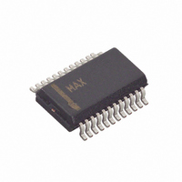
MAX6964AEG+T Maxim Integrated Products, MAX6964AEG+T Datasheet - Page 10

MAX6964AEG+T
Manufacturer Part Number
MAX6964AEG+T
Description
IC LED DRIVER LINEAR 24-QSOP
Manufacturer
Maxim Integrated Products
Type
Linear (I²C Interface)r
Datasheet
1.MAX6964AEG.pdf
(23 pages)
Specifications of MAX6964AEG+T
Topology
Open Drain, PWM
Number Of Outputs
17
Internal Driver
Yes
Type - Primary
Backlight, LED Blinker
Type - Secondary
RGB, White LED
Frequency
400kHz
Voltage - Supply
2 V ~ 3.6 V
Voltage - Output
7V
Mounting Type
Surface Mount
Package / Case
24-QSOP
Operating Temperature
-40°C ~ 125°C
Current - Output / Channel
50mA
Internal Switch(s)
Yes
Number Of Segments
12
Low Level Output Current
50 mA
Operating Supply Voltage
2 V to 3.6 V
Maximum Supply Current
122.1 uA
Maximum Power Dissipation
761 mW
Maximum Operating Temperature
+ 125 C
Mounting Style
SMD/SMT
Minimum Operating Temperature
- 40 C
Lead Free Status / RoHS Status
Lead free / RoHS Compliant
Efficiency
-
Lead Free Status / Rohs Status
Details
17-Output LED Driver/GPO with
Intensity Control and Hot-Insertion Protection
ing the MAX6964’s command byte by performing a
write (Figure 7). The master can now read n consecu-
tive bytes from the MAX6964 with the first data byte
being read from the register addressed by the initial-
ized command byte. When performing read-after-write
verification, remember to reset the command byte’s
address because the stored command byte address
has been autoincremented after the write (Table 2).
If the MAX6964 is operated on a 2-wire interface with
multiple masters, a master reading the MAX6964 should
use a repeated start between the write, which sets the
MAX6964’s address pointer, and the read(s) that takes
the data from the location(s) (Table 2). This is because it
is possible for master 2 to take over the bus after master
1 has set up the MAX6964’s address pointer but before
master 1 has read the data. If master 2 subsequently
changes the MAX6964’s address pointer, then master
1’s delayed read can be from an unexpected location.
The command address stored in the MAX6964 circu-
lates around grouped register functions after each data
byte is written or read (Table 2).
The reset input RST is an active-low input. When taken
low, RST clears any transaction to or from the MAX6964
on the serial interface and configures the internal regis-
ters to the same state as a power-up reset (Table 3).
The MAX6964 then waits for a START condition on the
serial interface.
On power-up, and whenever the RST input is pulled
low, all control registers are reset and the MAX6964
enters standby mode (Table 3). Power-up status makes
all outputs logic high (high impedance if external pullup
resistors are not fitted) and disables both the PWM
oscillator and blink functionality. The RST input can be
used as a hardware shutdown input, which effectively
turns off any LED (or other) loads and puts the device
into its lowest power condition.
The configuration register is used to configure the PWM
intensity mode and blink behavior, operate the O16 out-
put, and read back the BLINK input logic level (Table 4).
In blink mode, the outputs can be flipped between
using either the blink phase 0 registers or the blink
phase 1 registers. Flip control is both hardware (the
10
______________________________________________________________________________________
Command Address Autoincrementing
Operation with Multiple Masters
Detailed Description
Configuration Register
Initial Power-Up
Device Reset
Blink Mode
BLINK input) and software control (the blink flip flag B
in the configuration register) (Table 4).
The blink function can be used for LED effects by pro-
gramming different display patterns in the two sets of
output port registers, and using the software or hard-
ware controls to flip between the patterns.
If the blink phase 1 registers are written with 0xFF, then
the BLINK input can be used as a hardware disable to,
for example, instantly turn off an LED pattern pro-
grammed into the blink phase 0 registers. This tech-
nique can be further extended by driving the BLINK
input with a PWM signal to modulate the LED current to
provide fading effects.
The blink mode is enabled by setting the blink enable
flag E in the configuration register (Table 4). When blink
mode is enabled, the state of the blink flip flag and
BLINK input are EXORed to set the phase, and the out-
puts are set by either the blink phase 0 registers or the
blink phase 1 registers (Figure 11, Table 5).
The blink mode is disabled by clearing the blink enable
flag E in the configuration register (Table 4). When blink
mode is disabled, the state of the blink flip flag is
ignored, and the blink phase 0 registers alone control
the outputs.
The logic status of BLINK is made available as the read-
only blink status flag blink in the configuration register
(Table 4). This flag allows BLINK to be used as an extra
general-purpose input (GPI) in applications not using the
blink function. When BLINK is going to be used as a GPI,
blink mode should be disabled by clearing the blink
enable flag E in the configuration register (Table 4).
When the blink function is disabled, the two blink phase
0 registers set the logic levels of the 16 outputs (O0
through O15) (Table 6). A duplicate pair of registers
called the blink phase 1 registers are also used if the
blink function is enabled (Table 7). A logic high sets the
appropriate output high impedance, while a logic low
makes the port go low.
Reading a blink phase register reads the value stored
in the register, not the actual port condition. The port
output itself may or may not be at a valid logic level,
depending on the external load connected.
The 17th output, O16, is controlled through 2 bits in the
configuration register, which provide the same static or
blink control as the other 16 output ports.
Blink Phase Registers


