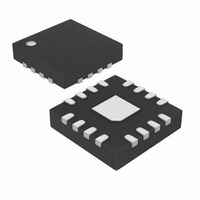
MAX6967ATE+ Maxim Integrated Products, MAX6967ATE+ Datasheet - Page 6

MAX6967ATE+
Manufacturer Part Number
MAX6967ATE+
Description
IC LED DRIVER LINEAR 16-TQFN
Manufacturer
Maxim Integrated Products
Type
Linear (Serial Interface)r
Datasheet
1.MAX6966ATE.pdf
(29 pages)
Specifications of MAX6967ATE+
Constant Current
Yes
Topology
Open Drain, PWM
Number Of Outputs
10
Internal Driver
Yes
Type - Primary
Backlight
Type - Secondary
RGB, White LED
Frequency
270kHz ~ 450kHz
Voltage - Supply
2.25 V ~ 3.6 V
Voltage - Output
7V
Mounting Type
Surface Mount
Package / Case
16-TQFN Exposed Pad
Operating Temperature
-40°C ~ 125°C
Current - Output / Channel
20mA
Internal Switch(s)
Yes
Number Of Segments
10
Low Level Output Current
21.1 mA
Operating Supply Voltage
2.25 V to 3.6 V
Maximum Supply Current
730 uA
Maximum Power Dissipation
1176 mW
Maximum Operating Temperature
+ 125 C
Mounting Style
SMD/SMT
Minimum Operating Temperature
- 40 C
Lead Free Status / RoHS Status
Lead free / RoHS Compliant
Efficiency
-
Lead Free Status / Rohs Status
Details
This section describes how to configure a MAX6966 or
MAX6967 on power-up.
Software engineers can use this section as a plain-text
guide to the device’s initialization routine. Hardware
engineers can use this section to get a quick overview
of the device’s capabilities and feature tradeoffs:
1) Before power-up, all 10 I/O ports P0 to P9 are high
2) After power-up, all 10 I/O ports P0 to P9 remain
3) Decide whether the DOUT/OSC pin will be used
10-Port Constant-Current LED Drivers and I/O
Expanders with PWM Intensity Control
6
QSOP
3–7,
9-13
impedance. They may be connected to inputs up to
+7V or loads connected to independent rails up to
+7V. The SPI bus inputs (SCLK, CS, DIN) are not
overvoltage protected, and must not be driven from
a voltage higher than V+.
high impedance. They may be connected to inputs
up to +7V or loads connected to V+ or independent
rails up to +7V. The ports are not configured as logic
inputs even though the ports are high impedance.
The device is in shutdown mode, and draws mini-
mum supply current regardless of I/O ports connec-
tions.
as SPI data output or PWM clock input, and
choose the MAX6966 or MAX6967 accordingly. If
14
15
16
—
_______________________________________________________________________________________
1
2
8
PIN
TQFN
7-11
PAD
1–5,
15
16
12
13
14
6
DOUT/OSC
Exposed
NAME
P0-P9
SCLK
GND
DIN
pad
CS
V+
Quick-Start Guide
Serial-Clock Input. On SCLK’s rising edge, data shifts into the internal shift register. On SCLK’s
falling edge, data is clocked out of DOUT. SCLK is active only while CS is low.
Chip-Select Input. Serial data is loaded into the shift register while CS is low. The most recent 16
bits of data latch on CS’s rising edge.
I/O Ports. P0 to P9 can be configured as open-drain current-sink outputs rated at 20mA
maximum, or as CMOS-logic inputs, or as open-drain logic outputs. Loads should be connected
to a supply voltage no higher than 7V.
Ground
Serial-Data Output. The data into DIN is valid at DOUT 15.5 clock cycles later. Use this pin to
daisy-chain several devices or allow data readback. Output is push-pull.
OSC Input. Apply a square-wave CMOS clock up to 100kHz as alternate PWM clock source.
The MAX6966 powers up with DOUT/OSC defaulting as DOUT output.
The MAX6967 powers up with DOUT/OSC defaulting as OSC input.
Serial-Data Input. Data from DIN loads into the internal 16-bit shift register on SCLK’s rising
edge.
Positive Supply Voltage. Bypass V+ to GND with a 0.1µF ceramic capacitor.
Exposed Pad on Package Underside. Connect to GND.
4) Allocate port functionality for the 10 I/O ports. All
5) Decide how to implement LED intensity control.
any ports are used as logic input, or if the applica-
tion needs read-after-write validation, then
DOUT/OSC needs to be configured as DOUT. Note
that both the MAX6966 and MAX6967 can configure
DOUT/OSC as either DOUT output or OSC clock
input; the only difference is the power-up default.
ports have the same features, so allocate ports for
either software convenience or board-routing rea-
sons. Any port can be constant-current LED drivers
(static or PWM), an open-drain logic output, or a
logic input. If fewer than 10 ports are used as con-
stant-current drivers, see the Applications
Information section for details on how to optimize the
PWM phasing to minimize load supply-current mod-
ulation.
The MAX6966/MAX6967 provide:
• Individual 8-bit PWM control per constant-current
• Individual 1-bit analog control (half/full) per
• Global 3-bit analog control, which applies to all
output
constant-current output
constant-current outputs
FUNCTION
Pin Description


