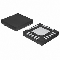
MAX16806ATP+ Maxim Integrated Products, MAX16806ATP+ Datasheet - Page 5

MAX16806ATP+
Manufacturer Part Number
MAX16806ATP+
Description
IC LED DRIVR HIGH BRIGHT 20-TQFN
Manufacturer
Maxim Integrated Products
Type
HBLED Driverr
Datasheet
1.MAX16805ATP.pdf
(19 pages)
Specifications of MAX16806ATP+
Constant Current
Yes
Topology
PWM
Number Of Outputs
1
Internal Driver
Yes
Type - Primary
Automotive
Type - Secondary
High Brightness LED (HBLED)
Frequency
400kHz
Voltage - Supply
5.5 V ~ 40 V
Voltage - Output
5.1V
Mounting Type
Surface Mount
Package / Case
20-TQFN Exposed Pad
Operating Temperature
-40°C ~ 125°C
Current - Output / Channel
350mA
Internal Switch(s)
Yes
Operating Supply Voltage
5.5 V to 40 V
Maximum Power Dissipation
2758.6 mW
Maximum Operating Temperature
+ 125 C
Mounting Style
SMD/SMT
Minimum Operating Temperature
- 40 C
Lead Free Status / RoHS Status
Lead free / RoHS Compliant
Efficiency
-
Lead Free Status / Rohs Status
Details
ELECTRICAL CHARACTERISTICS (continued)
(V
SW = CFD = Open, T
Note 1: All devices 100% production tested at T
Note 2: Resistors were added from OUT to CS+ to aid with the power dissipation during testing.
Note 3: Dropout is measured as follows: Connect a resistor from OUT to CS+. Connect R
Note 4: t
Note 5: TPF/SCL (SCL for MAX16805) and TPN/SDA (SDA for the MAX16805) are I
Note 6: C
EEPROM
V
Programming
EEPROM Data-Retention Time
I
Logic Input-Voltage High
Logic Input-Voltage Low
Input Capacitance
SDA Output Voltage Low
I
Serial Clock Frequency
Bus Free Time Between STOP
and START Condition
START Condition Hold Time
Clock Low Period
Clock High Period
Repeat START Condition Setup
Time
Data Hold Time
Data Setup Time
Receive SCL/SDA Rise Time
Receive SCL/SDA Fall Time
STOP Condition Setup Time
Pulse Width of Spike Suppressed
Transmit SDA Fall Time
2
2
IN
IN
C DIGITAL INPUTS (TFP/SCL, TFN/SDA) (Note 5)
C INTERFACE TIMING (Figure 1)
Voltage for EEPROM
= V
EEPROM-Programmable, High-Voltage, 350mA
EN
V
I
MAX16805/MAX16806 are the only parts on the bus for production programming.
ON
OUT
OUT
B
PARAMETER
= 12V, C
is the total bus capacitance.
time includes the delay and the rise time needed for I
to drop below 10%. See the Typical Operating Characteristics . t
+3V (record V
_______________________________________________________________________________________
V5
A
= T
LED Drivers with LED Current Foldback
= 0.1µF, I
J
= -40°C to +125°C, unless otherwise noted. Typical values are at T
OUT
as V
V5
= 0, CS- = GND, R
OUT1
SYMBOL
t
t
t
t
t
HD:DAT
HD:STA
SU:STA
SU:DAT
SU:STO
t
t
t
f
HIGH
V
LOW
V
BUF
V
SCL
t
t
t
SP
). Reduce V
OL
R
IH
IL
F
J
= +25°C. Limits over the operating temperature range are guaranteed by design.
I
A master device must provide a hold time
of at least 300ns for the SDA signal
(referred to V
to bridge the undefined region of SCL’s
falling edge
I
SINK
SINK
IN
until V
SENSE
= 3mA
< 6mA, C
OUT
= 0.56Ω, V
IL
CONDITIONS
OUT
B
of the SCL signal) in order
= 0.97 x V
≤ 400pF (Note 6)
to reach 90% of its final value. t
DIM
OUT1
ON
= 4V, DGND = GND, TFP/SCL = 5V, TFN/SDA = 0V,
and t
(record as V
2
C interface compatible only when the
OFF
SENSE
are tested with 13Ω from OUT to CS+.
A
IN2
= 0.56Ω from CS+ to CS-. Set V
= +25°C.) (Note 1)
MIN
100
2.8
1.3
0.6
1.3
0.6
0.6
0.6
20
10
and V
0
OFF
OUT2
time is the time needed for
TYP
22
50
5
). ΔV
DO
MAX
400
300
250
250
0.8
0.4
0.9
24
= V
IN2
- V
UNITS
Years
kHz
IN
pF
OUT2
µs
µs
µs
µs
µs
µs
ns
ns
ns
µs
ns
ns
V
V
V
V
=
5
.


