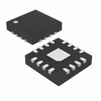
MAX6947ATE+T Maxim Integrated Products, MAX6947ATE+T Datasheet - Page 17

MAX6947ATE+T
Manufacturer Part Number
MAX6947ATE+T
Description
IC LED DRIVER LINEAR 16-TQFN
Manufacturer
Maxim Integrated Products
Type
Linear (I²C Interface)r
Datasheet
1.MAX6947ATE.pdf
(24 pages)
Specifications of MAX6947ATE+T
Constant Current
Yes
Topology
Open Drain, PWM
Number Of Outputs
10
Internal Driver
Yes
Type - Primary
Backlight
Type - Secondary
RGB, White LED
Frequency
400kHz
Voltage - Supply
2.25 V ~ 3.6 V
Voltage - Output
7V
Mounting Type
Surface Mount
Package / Case
16-TQFN Exposed Pad
Operating Temperature
-40°C ~ 125°C
Current - Output / Channel
20mA
Internal Switch(s)
Yes
Number Of Segments
3
Low Level Output Current
21.12 mA
Operating Supply Voltage
2.25 V to 3.6 V
Maximum Supply Current
60 uA
Maximum Power Dissipation
1176 mW
Maximum Operating Temperature
+ 125 C
Mounting Style
SMD/SMT
Minimum Operating Temperature
- 40 C
Lead Free Status / RoHS Status
Lead free / RoHS Compliant
Efficiency
-
Lead Free Status / Rohs Status
Details
Table 10. MAX6946/MAX6947 Slave
Addresses
Both SCL and SDA remain high when the interface is
not busy. A master signals the beginning of a transmis-
sion with a START (S) condition by transitioning SDA
from high to low while SCL is high. When the master fin-
ishes communicating with the slave, it issues a STOP
(P) condition by transitioning SDA from low to high
while SCL is high. The bus is then free for another
transmission (Figure 9).
One data bit is transferred during each clock pulse.
The data on SDA must remain stable while SCL is high
(Figure 10).
Any bytes received after the command byte are data
bytes. The first data byte goes into the internal register
of the MAX6946/MAX6947 selected by the command
byte (Figure 11). If multiple data bytes are transmitted
before a STOP condition is detected, these bytes are
generally stored in subsequent MAX6946/MAX6947
internal registers because the command byte autoin-
crements (Table 1).
Read from the MAX6946/MAX6947 using the
MAX6946/MAX6947s’ internally stored command byte
as an address pointer the same way the stored com-
mand byte is used as an address pointer for a write.
The pointer autoincrements after each data byte is read
using the same rules as for a write (Table 1). Thus, a
read is initiated by first configuring the MAX6946/
MAX6947s’ command byte by performing a write
(Figures 12 and 13). The master can now read n con-
AD0 = GND
AD0 = V
MAX6947
MAX6946
DD
10-Port, Constant-Current LED Driver and
I/O Expander with PWM Intensity Control
______________________________________________________________________________________
Message Format for Reading
Start and Stop Conditions
SLAVE ADDRESS
010 0000
010 0100
010 0000
Acknowledge
Bit Transfer
secutive bytes from the MAX6946/MAX6947 with the
first data byte being read from the register addressed
by the initialized command byte (Figure 14). When per-
forming read-after-write verification, remember to reset
the command byte’s address because the stored com-
mand byte address has been autoincremented after
the write (Table 1).
Figure 9. Start and Stop Conditions
Figure 10. Bit Transfer
Figure 11. Acknowledge
TRANSMITTER
SDA
SCL
SDA
SCL
RECEIVER
CONDITION
SDA BY
SDA BY
START
SCL
S
CONDITION
START
DATA LINE STABLE;
S
DATA VALID
1
CHANGE OF DATA
ALLOWED
2
FOR ACKNOWLEDGE
CLOCK PULSE
8
CONDITION
9
STOP
P
17


