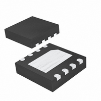
MAX1848ETA+T Maxim Integrated Products, MAX1848ETA+T Datasheet - Page 2

MAX1848ETA+T
Manufacturer Part Number
MAX1848ETA+T
Description
IC LED DRIVR WHITE BCKLGT 8-TDFN
Manufacturer
Maxim Integrated Products
Type
Backlight, White LEDr
Datasheet
1.MAX1848ETAT.pdf
(9 pages)
Specifications of MAX1848ETA+T
Constant Current
Yes
Topology
PWM, Step-Up (Boost)
Number Of Outputs
1
Internal Driver
Yes
Type - Primary
Backlight
Type - Secondary
White LED
Frequency
1MHz ~ 1.5MHz
Voltage - Supply
2.6 V ~ 5.5 V
Mounting Type
Surface Mount
Package / Case
8-TDFN Exposed Pad
Operating Temperature
-40°C ~ 85°C
Current - Output / Channel
500mA
Internal Switch(s)
Yes
Efficiency
87%
Number Of Segments
3
Operating Supply Voltage
2.6 V to 5.5 V
Maximum Power Dissipation
1951 mW
Maximum Operating Temperature
+ 85 C
Mounting Style
SMD/SMT
Minimum Operating Temperature
- 40 C
Lead Free Status / RoHS Status
Lead free / RoHS Compliant
Voltage - Output
-
Lead Free Status / Rohs Status
Details
ABSOLUTE MAXIMUM RATINGS
V+ to GND ................................................................-0.3V to +6V
PGND to GND .......................................................-0.3V to +0.3V
LX, OUT to GND .....................................................-0.3V to +14V
LX to OUT ...............................................................-14V to +0.3V
CTRL to GND.......................................-0.3V to +6V or (V+ + 2V)
COMP, CS to GND .......................................-0.3V to (V+ + 0.3V)
LX Current ....................................................................0.45A
DC ELECTRICAL CHARACTERISTICS
(V+ = 3V, V
noted. Typical values are at T
White LED Step-Up Converter in SOT23
Stresses beyond those listed under “Absolute Maximum Ratings” may cause permanent damage to the device. These are stress ratings only, and functional
operation of the device at these or any other conditions beyond those indicated in the operational sections of the specifications is not implied. Exposure to
absolute maximum rating conditions for extended periods may affect device reliability.
2
ERROR AMPLIFIER
OSCILLATOR
Supply Voltage
Undervoltage Lockout Threshold
Quiescent Current
Shutdown Supply Current
Overvoltage Threshold
OUT Input Bias Current
Output Voltage Range
CTRL to CS Regulation
CS Input Bias Current
CTRL Input Resistance
CTRL Dual Mode Threshold
CS Line Regulation
COMP Pin Resistance to Ground
COMP Output Voltage Swing
Operating Frequency
Minimum Duty Cycle
Maximum Duty Cycle
_______________________________________________________________________________________
PARAMETER
OUT
= 11V, L = 33µH, C
A
= +25°C.)
OUT
V+ rising, 40mV hysteresis typical
V+ falling
Not switching, V
Switching, V
V
V+ rising, 1V hysteresis typical
V+ falling
V
V
V
Hysteresis = 25mV typical
V+ = 2.6V to 5.5V, V
Device in shutdown or overvoltage
PWM mode
Pulse skipping
V
= 1µF, C
CTRL
OUT
CTRL
CS
CTRL
= V
= 13V
= GND
= 2V, V+ = 2.6V to 5.5V
= V+, V
CTRL
COMP
CTRL
/13.33
CS
= 0.15µF, R
CTRL
= GND
= V+, V
RMS
CONDITIONS
CTRL
= V
CS
CS
= 3V
SENSE
= V+
T
T
V
V
= GND
Continuous Power Dissipation (T
Operating Temperature Range ...........................-40°C to +85°C
Junction Temperature ......................................................+150°C
Storage Temperature Range .............................-60°C to +150°C
Lead Temperature (soldering, 10s) .................................+300°C
A
A
CTRL
CTRL
8-Pin SOT23 (derate 9.7mW/°C above +70°C).............777mW
8-Pin Thin QFN 3mm
above +70°C)..............................................................1951mW
= +25°C
= +85°C
= 5Ω, V
> 0.25V
= GND
CTRL
= 1V, T
✕
3mm (derate 24.4mW/°C
V
A
2.15
2.10
12.5
11.5
V+ -
D IOD E
MIN
450
100
2.6
7.5
0.3
1.0
=
10
71
85
0° ° C to +85° ° C, unless otherwise
A
= +70°C)
13.25
12.25
TYP
2.38
2.34
0.25
0.01
0.01
0.05
670
170
0.3
0.3
1.2
20
75
15
12
90
1
0
MAX
1100
2.59
2.56
0.40
14.0
12.5
240
5.5
2.4
1.5
13
30
81
50
97
2
1
1
1
UNITS
mV/V
MHz
%/V
mA
mV
µA
µA
µA
kΩ
kΩ
%
%
V
V
V
V
V


