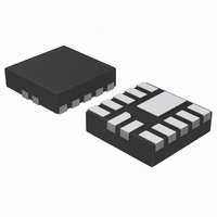
NCP5623CMUTBG ON Semiconductor, NCP5623CMUTBG Datasheet

NCP5623CMUTBG
Specifications of NCP5623CMUTBG
Available stocks
Related parts for NCP5623CMUTBG
NCP5623CMUTBG Summary of contents
Page 1
... G = Pb−Free Package (Note: Microdot may be in either location) ORDERING INFORMATION Device Package Shipping NCP5623CMUTBG LLGA12 3000/Tape & Reel (Pb−Free) †For information on tape and reel specifications, including part orientation and tape sizes, please refer to our Tape and Reel Packaging Specification Brochure, BRD8011/D. ...
Page 2
Vbat 1 mF/6 GND Vbat AGND 6 DIGITAL CONTROL SDA 7 SCL 9 Vbat R1 ANALOG GND 8 FUNCTIONS 62 k Figure 2. Simplified Block Diagram C3 220 NCP5623C CHARGE PUMP DC/DC CONVERTER OVER ...
Page 3
PIN ASSIGNMENT PIN Name Type 1 C1P POWER One side of the external charge pump capacitor (C pin 12 (Note 1). 2 GND POWER This pin is the GROUND signal for the analog and digital blocks and must be connected ...
Page 4
MAXIMUM RATINGS Symbol V Power Supply (see Figure 3) BAT Vout Output Power Supply SDA, SCL, Digital Input Voltage SHDI2C Digital Input Current ESD Human Body Model 1500 100 pF (Note 3) Machine Model LLGA12 ...
Page 5
POWER SUPPLY SECTION: (Typical values are referenced +25°C, Min & Max values are referenced −40°C to +85°C ambient temperature, unless otherwise A noted), operating conditions 2.85 V < Vbat < 5.5 V, unless otherwise noted. Pin Symbol ...
Page 6
ANALOG SECTION: (Typical values are referenced +25°C, Min & Max values are referenced −40°C to +85°C ambient temperature, unless otherwise A noted), operating conditions 2.85 V < Vbat < 5.5 V, unless otherwise noted. Pin Symbol 8 ...
Page 7
DC/DC OPERATION The converter is based on a charge pump technique to generate a DC voltage capable to supply the RGB LED load. The system regulates the current flowing into each LED, not the DC Vout value, by means of ...
Page 8
Byte#1 : I2C Physical Address, based 7 bits : % 011 1001 ³ $ Byte#2 : DATA register RLED2 RLED1 RLED0 *Note: according to the I2C specifications, the physical address is based on ...
Page 9
The dimming is built with 30 steps and the time delay encoded into the second byte of the I2C transaction: see Table 1. When the gradual dimming is deactivated ( 1), the output current ...
Page 10
Step Figure 4. Output Current Programmed Value ( ILED = F(Step) ) 100 Figure 5. NCP5623C Typical Efficiency as a Function of ...
Page 11
... 0.05 C NOTE 3 *For additional information on our Pb−Free strategy and soldering details, please download the ON Semiconductor Soldering and Mounting Techniques Reference Manual, SOLDERRM/D. N. American Technical Support: 800−282−9855 Toll Free USA/Canada Europe, Middle East and Africa Technical Support: Phone: 421 33 790 2910 Japan Customer Focus Center Phone: 81− ...


