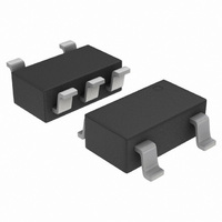
NCP5007SNT1G ON Semiconductor, NCP5007SNT1G Datasheet

NCP5007SNT1G
Specifications of NCP5007SNT1G
NCP5007SNT1GOSTR
Available stocks
Related parts for NCP5007SNT1G
NCP5007SNT1G Summary of contents
Page 1
... View) ORDERING INFORMATION Device Package Shipping NCP5007SNT1 TSOP−5 3000/Tape & Reel NCP5007SNT1G TSOP−5 3000/Tape & Reel (Pb−Free) †For information on tape and reel specifications, including part orientation and tape sizes, please refer to our Tape and Reel Packaging Specifications Brochure, BRD8011/D. ...
Page 2
Thermal Shutdown EN 3 100 k GND − 300 k +200 mV Band Gap Figure 2. Block Diagram NCP5007 Current Sense Vsense CONTROLLER GND http://onsemi.com 2 V bat V 5 bat V 4 out Q1 GND 2 ...
Page 3
PIN FUNCTION DESCRIPTION Pin Symbol Type 1 FB ANALOG This pin provides the output current range adjustment by means of a sense resistor connected INPUT to the analog control or with a PWM control. The dimming function can be achieved ...
Page 4
MAXIMUM RATINGS Rating Power Supply Output Power Supply Voltage Compliance Digital Input Voltage Digital Input Current ESD Capability (Note 1) Human Body Model (HBM) Machine Model (MM) TSOP5 Package Power Dissipation @ T = +85°C (Note 2) A Thermal Resistance, ...
Page 5
ANALOG SECTION (Typical values are referenced to T temperature, unless otherwise noted.) Rating High Level Input Voltage Low Level Input Voltage EN Pull Down Resistor Feedback Voltage Threshold Output Current Stabilizes @ 5% time delay following a = 3.6 V, ...
Page 6
Basically, the chip operates with two cycles: Cycle #1 : time t1, the energy is stored into the inductor Cycle #2 : time t2, the energy is dumped to the load The POR signal sets the flip−flop and the first ...
Page 7
LED 1000 2 LED 800 5 LED 600 400 200 out bat (V) bat Figure 5. Maximum Output Power as a Function of the Battery Supply Voltage ...
Page 8
Output Current Range Set−Up The current regulation is achieved by means of an external sense resistor connected in series with the LED string The current flowing through the LED creates a voltage drop across the sense resistor R1. ...
Page 9
Output Load Drive In order to take advantage of the built−in Boost capabilities, one shall operate the NCP5007 in the continuous output current mode. Such a mode is achieved by using and external reservoir capacitor (see Table 1) across the ...
Page 10
TYPICAL OPERATING CHARACTERISTICS (All curve conditions mH, Cin = 4.7 mF, C 100 2 LED/ LED/ LED/ LED/ 2.50 3.00 ...
Page 11
TYPICAL OPERATING CHARACTERISTICS (All curve conditions mH, Cin = 4.7 mF, C 1.4 1.2 1.0 0.8 0.6 0.4 0.2 0.0 2.7 3.3 3.9 4 BATTERY VOLTAGE (V) bat Figure 20. Standby Current ...
Page 12
NCP5007 TYPICAL OPERATING WAVEFORMS = 22 mH, 5 LED, I Conditions 3 bat out Figure 23. Typical Power Up Response V out Inductor Current = 22 mH, 5 LED, I Conditions 3 ...
Page 13
NCP5007 TYPICAL OPERATING WAVEFORMS = 22 mH, 5 LED, I Conditions 3 bat out Figure 25. Typical Inductor Current = 22 mH, 5 LED, I Conditions 3 bat out Figure 26. Typical ...
Page 14
NCP5007 TYPICAL OPERATING WAVEFORMS Test Conditions mH mA, V out Figure 27. Typical Output Peak Voltage http://onsemi.com 14 Output Voltage Inductor Current = 3.6 V, Ambient Temperature, LED = 5 bat ...
Page 15
TYPICAL APPLICATIONS CIRCUITS Standard Feedback The standard feedback provides constant current to the LEDs, independently of the V supply and number of bat GND R1 GND 15 W Figure 28. Basic DC Current Mode Operation with PWM Operation The analog ...
Page 16
Average Network R2 PWM 150 k GND NOTE: RC filter R2 and C3 is optional (see text) Figure 29. Basic DC Current Mode Operation with PWM Control To implement such a function, lets consider the feedback input as an operational ...
Page 17
Typical LEDs Load Mapping Since the output power is battery limited (see Figure 5), one can arrange the LEDs in a variety of different 50 mA Load D1 LED D2 LED D3 LED D4 LED Sense R1 3.9 W Resistor ...
Page 18
... ON Semiconductor provides a demo board to evaluate the performance of the NCP5007. The schematic for that demo board is illustrated in Figure 32. V bat SELECT MANUAL BRIGHTNESS 1 MODULATION R1 J3 150 k GND C2 V 100 nF bat PWR J1 GND V bat 1 2 Figure 32. NCP5007 Demo Board Schematic Diagram NCP5007 TP3 ...
Page 19
... Manufacturer 30 V Low Vf Schottky Diode ON Semiconductor 20 V Low Vf Schottky Diode ON Semiconductor 20 V Low Vf Schottky Diode ON Semiconductor Ceramic Cap. 1.0 mF/16 V Ceramic Cap. 4.7 mF/6.3 V Inductor 22 mH Inductor 22 mH Figure 33. NCP5007 Demo Board PCB: Top Layer Figure 34. NCP5007 Demo Board Top Silkscreen ...
Page 20
FIGURES INDEX Figure 1: Typical Application . . . . . . . . . . . . . . . . . . . . . . . . . . . . . . . . . . ...
Page 21
... H *For additional information on our Pb−Free strategy and soldering details, please download the ON Semiconductor Soldering and Mounting Techniques Reference Manual, SOLDERRM/D. ON Semiconductor and are registered trademarks of Semiconductor Components Industries, LLC (SCILLC). SCILLC reserves the right to make changes without further notice to any products herein ...


