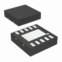
LM2791LD-L/NOPB National Semiconductor, LM2791LD-L/NOPB Datasheet - Page 4

LM2791LD-L/NOPB
Manufacturer Part Number
LM2791LD-L/NOPB
Description
IC LED DRIVR WHITE BCKLGT 10-LLP
Manufacturer
National Semiconductor
Type
Backlight, White LEDr
Datasheet
1.LM2791LD-LNOPB.pdf
(11 pages)
Specifications of LM2791LD-L/NOPB
Constant Current
Yes
Topology
PWM, Switched Capacitor (Charge Pump)
Number Of Outputs
2
Internal Driver
Yes
Type - Primary
Backlight
Type - Secondary
White LED
Frequency
450kHz ~ 850kHz
Voltage - Supply
3 V ~ 5.8 V
Mounting Type
Surface Mount
Package / Case
10-LLP
Operating Temperature
-30°C ~ 85°C
Current - Output / Channel
36mA
Internal Switch(s)
Yes
Operating Supply Voltage (typ)
3.3/5V
Number Of Segments
2
Operating Temperature (min)
-30C
Operating Temperature (max)
85C
Operating Temperature Classification
Commercial
Package Type
LLP EP
Pin Count
10
Mounting
Surface Mount
Power Dissipation
400mW
Operating Supply Voltage (min)
3V
Operating Supply Voltage (max)
5.8V
Lead Free Status / RoHS Status
Lead free / RoHS Compliant
Voltage - Output
-
Efficiency
-
Lead Free Status / Rohs Status
Compliant
Other names
LM2791LD-L
LM2791LD-LTR
LM2791LD-LTR
Available stocks
Company
Part Number
Manufacturer
Quantity
Price
Company:
Part Number:
LM2791LD-L/NOPB
Manufacturer:
BOSCH
Quantity:
6 222
www.national.com
I
I
I
I
I
I
V
V
I
R
I
f
t
DX
Dx
DX
D-MATCH
Q
SD
LEAK-SD
SET
SW
START
IH
IL
BRGT
Absolute Maximum Ratings
If Military/Aerospace specified devices are required,
please contact the National Semiconductor Sales Office/
Distributors for availability and specifications.
Electrical Characteristics
Limits in standard typeface are for T
Unless otherwise specified, C
Note 1: Absolute maximum ratings indicate limits beyond which damage to the device may occur. Electrical specifications do not apply when operating the device
beyond its rated operating conditions.
Note 2: D1 and D2 may be shorted to GND without damage. P
Note 3: In the test circuit, all capacitors are 1.0µF, 0.3Ω maximum ESR capacitors. Capacitors with higher ESR will increase output resistance, reduce output
voltage and efficiency.
Note 4: The output switches operate at one half of the oscillator frequency, f
Note 5: The interanl thresholds of the shutdown bar are set at about 40% of V
Note 6: This electrical specification is guaranteed by design.
Note 7: For more inforamtion regarding the LLP package, please refer to National Semiconductor Application note AN1187
Symbol
V
BRGT, SD
Power Dissipation(Note 2)
T
θ
Storge Temperature
Lead Temp. (Soldering, 5 sec.)
JA
JMAX
IN
(Note 7)
(Note 2)
Diode Current at ID1,2
Available Current at Output Dx
Load Regulation at Output Dx
Line Regulation of Dx Output
Current
Current Matching Between Any
Two Outputs
Quiescent Supply Current
Shutdown Supply Current
SD Input Logic High
SD Input Logic Low
SD Input Leakage Current
BRGT Input Resistance
I
Switching Frequency (Note 4)
Startup Time(Note 6)
SET
Pin Output Current
Parameter
1
= C
IN
J
= C
= 25˚C and limits in boldface type apply over the full Operating Temperature Range.
-0.3 to (V
−65˚C to +100˚C
HOLD
= 1 µF, V
−0.3 to 6V
V
V
V
V
V
V
V
V
3.3V ≤ V
V
3.0V ≤ V
V
3.0V ≤ V
Load Current
3.0V ≤ V
85˚C
3.0V ≤ V
3.0V ≤ V
0V ≤ V
3.0V ≤ V
I
(Note 1)
Dx
IN
IN
IN
IN
IN
IN
IN
DX
DX
DX
D1
400 mW
OUT
55˚C/W
= 3V, R
= 3V
= 3.3V
= 3.6V
= 90% steady state
+0.2V)
, V
= 4.4V
=3.6V
=3.0V
=4.0V
150˚C
260˚C
= 3.6V
may be shorted to GND for 1sec without damage.
D2
SD
IN
IN
IN
IN
IN
IN
IN
IN
= 3.6V
≤ V
Conditions
SET
≤ 4.4V
≤ 4.4V
≤ 4.4V, Active, No
≤ 5.5V, Shutdown at
≤ 5.5V, (Note 5)
≤ 5.5V, (Note 5)
≤ 4.4V
= 3.6V, V
OSC
IN
IN
4
= 270Ω
.
= 2f
Operating Conditions
SW
ESD Rating
Human Body Model
Machine Model
Input Voltage (V
BRGT
Ambient Temperature (T
Junction Temperature (T
DIODE
.
= 3.6V, R
IN
0.8V
SET
16.5
12.8
13.3
)
Min
450
= 332Ω, BRGT pin = 0V.
IN
A
J
)
)
I
Dx
14.5
15.1
15.7
16.8
15.4
15.7
Typ
250
650
0.3
0.7
0.1
0.3
0.1
18
16
10
/25
0.2V
−30˚C to +100˚C
Max
17.7
18.4
−30˚C to +85˚C
850
2
1
3.0V to 5.8V
IN
0 to 3.0V
200V
Units
2KV
kHz
mA
mA
mA
mA
mA
µA
µA
kΩ
µs
%
V
V


