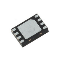
LDS8711 IXYS, LDS8711 Datasheet

LDS8711
Specifications of LDS8711
Related parts for LDS8711
LDS8711 Summary of contents
Page 1
... The supply voltage down to 2.7 V for new Li-ion battery chemistries or two alkaline battery cells extends the battery life. Under-voltage protection disables the part when V voltage reaches 2 The LDS8711 has thermal shutdown set at 150 Above this value , the switching. The part resumes normal operations when temperature drops below 130 The over-current protection provides cycle-by-cycle current limit ...
Page 2
... LDS8711 ABSOLUTE MAXIMUM RATINGS Parameter V voltage SW, LEDS, Vh voltage OUT EN/SET voltage LED Current Storage Temperature Range Junction Temperature Range 8-pin TDFN package Thermal Resistance Soldering Temperature RECOMMENDED OPERATING CONDITIONS Parameter V IN Ambient Temperature Range Typical application circuit with external components is shown on page 1. ...
Page 3
... LDS8711 Smart OneWire™ TIMING SPECIFICATION Parameter t EN/PWM setup from shutdown to PWM mode SETUP1 t EN/SET setup from shutdown to Smart OneWire™ Interface mode SETUP2 t Bit “zero” positive pulse BO t Bit “one” positive pulse B1 t Low time between command pulses or two command sets ...
Page 4
... LDS8711 TYPICAL CHARACTERISTICS Vin = 3.6V 30mA (10 LEDs per string), C OUT Power Efficiency vs. Input Voltage LED Current vs. PWM Duty Cycle Soft Start Waveforms Ch 1 (yellow) – EN pin (green) – SW node voltage Ch 3 (red) – Inductor current (blue © 2010 IXYS Corp. Characteristics subject to change without notice = 1 μ ...
Page 5
... LDS8711 TYPICAL CHARACTERISTICS Vin = 3.6V 30mA (10 LEDs per string), C OUT Waveforms at PWM LED Current Regulation Ch 1 (yellow) – PWM signal at 1 kHz 5% duty cycle C2 (green) – SW node voltage, Ch 3(red) – LED Current. Ch4 (blue OUT Waveforms at PWM LED Current Regulation Ch 1 (yellow) – PWM signal at 30 kHz 25% duty cycle C2 (green) – ...
Page 6
... LDS8711 PIN DESCRIPTION Pin # Name 1 V Input Voltage, connect to battery or power supply IN 2 GND Analog Ground 3 PGND Power Ground 4 SW Switch input; Connect inductor terminal to this pin Output voltage; Connect to the LED string anode 5 V OUT terminal to this pin. High Voltage Bypass; Connect a 0.01 µF capacitor ...
Page 7
... IXYS Corp. Characteristics subject to change without notice Figure 3. LDS8711 Functional Block Diagram The LDS8711 has soft start function that prevent high input current spike at device’ wake-up. The EN/PWM pin should be held low for more than completely turn device in low current SETUP1, shutdown mode ...
Page 8
... Figure 2). If LDS8711 is not able recognize command due some error in programming or transmit, it will go in shutdown mode after 10 ms timeout Once in PWM mode, LDS8711 is not able recognize Smart OneWire™ Interface commands and requires restart to reprogram LED current. Protection Mode The output voltage V ...
Page 9
... LDS8711 We recommend C in the range 1.0 – 2.2 µF to OUT achieve better efficiency and driver’s stability. Recommended Layout In active mode, the driver switches internally at a high frequency. We recommend minimize trace length to all external capacitors and inductor. The input and output ceramic capacitors (X5R or X7R type) should located as close to the device’ ...
Page 10
... LDS8711 PACKAGE DRAWING AND DIMENSIONS 8-PIN TDFN, 2mm x 3mm, 0.5mm PITCH SYMBOL MIN NOM A 0.700 0.750 A1 - 0.000 A2 0.203 Ref. b 0.180 0.230 D 2.950 3.000 D1 1.750 1.800 E 1.950 2.000 E1 1.550 1.600 e 0.500 Bsc L 0.350 0.400 Note: 1. All dimensions are in millimeters 2. Complies with JEDEC Standard MO-220 © ...
Page 11
... All packages are RoHS-compliant (Lead-free, Halogen-free). 2) The standard lead finish is Matte-Tin. 3) The device used in the above example is a LDS8711 XXX–T2-300 (2x3 TDFN, Tape & Reel LED Current). 4) For additional package and current options, please contact your nearest IXYS Corp. Sales office. © 2010 IXYS Corp. ...
Page 12
... LDS8711 Warranty and Use IXYS CORP. MAKES NO WARRANTY, REPRESENTATION OR GUARANTEE, EXPRESS OR IMPLIED, REGARDING THE SUITABILITY OF ITS PRODUCTS FOR ANY PARTICULAR PURPOSE, NOR THAT THE USE OF ITS PRODUCTS WILL NOT INFRINGE ITS INTELLECTUAL PROPERTY RIGHTS OR THE RIGHTS OF THIRD PARTIES WITH RESPECT TO ANY PARTICULAR USE OR APPLICATION AND SPECIFICALLY DISCLAIMS ANY AND ALL LIABILITY ARISING OUT OF ANY SUCH USE OR APPLICATION, INCLUDING BUT NOT LIMITED TO, CONSEQUENTIAL OR INCIDENTAL DAMAGES ...


