ADP8860ACBZ-R7 Analog Devices Inc, ADP8860ACBZ-R7 Datasheet
ADP8860ACBZ-R7
Specifications of ADP8860ACBZ-R7
Available stocks


Related parts for ADP8860ACBZ-R7


ADP8860ACBZ-R7 Summary of contents
Page 1
FEATURES Charge pump with automatic gain selection of 1×, 1.5×, and 2× for maximum efficiency Up to two built-in comparator inputs with programmable modes for ambient light sensing Outdoor, office, and dark modes for maximum backlight power savings 7 independent ...
Page 2
ADP8860 TABLE OF CONTENTS Features .............................................................................................. 1 Applications ....................................................................................... 1 General Description ......................................................................... 1 Typical Operating Circuit ................................................................ 1 Revision History ............................................................................... 2 Specifications ..................................................................................... Timing Diagram ..................................................................... 5 Absolute Maximum Ratings ............................................................ 6 Maximum Temperature ...
Page 3
SPECIFICATIONS VIN = 3.6 V, SCL = 2.7 V, SDA = 2.7 V, nINT = open, nRST = 2.7 V, CMP_IN = typical values are 25°C and are not guaranteed, minimum and maximum limits ...
Page 4
ADP8860 Parameter AMBIENT LIGHT SENSING COMPARATORS Ambient Light Sensor Current DAC Bit Step Threshold L2 Level Threshold L3 Level FAULT PROTECTION Startup Charging Current Source Output Voltage Threshold Exit Soft Start Short-Circuit Protection Output Overvoltage Protection Activation Level OVP Recovery ...
Page 5
I C TIMING DIAGRAM SDA t LOW SCL START CONDITION Sr = REPEATED START CONDITION P = STOP CONDITION SU, DAT t t HIGH SU, STA t Sr HD, ...
Page 6
ADP8860 ABSOLUTE MAXIMUM RATINGS Table 2. Parameter VIN, VOUT D1, D2, D3, D4, D5, D6, and D7 CMP_IN nINT, nRST, SCL, and SDA Output Short-Circuit Duration Operating Ambient Temperature Range Operating Junction Temperature Range Storage Temperature Range Soldering Conditions ESD ...
Page 7
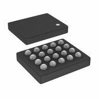
PIN CONFIGURATIONS AND FUNCTION DESCRIPTIONS PIN 1 INDICATOR ADP8860 D1 3 TOP VIEW SCL 4 (Not to Scale) nRST 5 NOTES 1. CONNECT THE EXPOSED PADDLE TO GND1 AND/OR GND2. Figure 3. LFCSP Pin Configuration Table ...
Page 8
ADP8860 TYPICAL PERFORMANCE CHARACTERISTICS VIN = 3.6 V, SCL = 2.7 V, SDA = 2.7 V, nRST = 2 otherwise noted. 2 LOAD OUT 1.8 1.6 1.4 1.2 1.0 0.8 0.6 0.4 0.2 0 1.5 ...
Page 9
30mA D1: 0.2 0.4 0.6 0.8 1.0 1.2 V (V) HR Figure 11. Typical Diode Current vs. Current Sink Headroom Voltage ( ...
Page 10
ADP8860 1.4 1.3 1.2 1.1 1.0 0.9 0.8 0.7 2.5 3.0 3.5 4.0 V (V) IN Figure 17. Typical ALS Current GAIN = 2× 5 10mA OUT 5.3 5.2 5.1 5.0 4.9 ...
Page 11
T V (AC-COUPLED) 50mV/DIV (AC-COUPLED) 50mV/DIV OUT 2 I (AC-COUPLED) 10mA/DIV 1µ 1µ 1µ 1µF IN OUT 120mA OUT Figure 23. ...
Page 12
ADP8860 THEORY OF OPERATION The ADP8860 combines a programmable backlight LED charge pump driver with automatic phototransistor control. This combi- nation allows for significant power savings because it is able to change the current intensity based on the lighting conditions. ...
Page 13
POWER STAGE Because typical white LEDs require drive them, some form of boosting is required over the typical variation in battery voltage. The ADP8860 accomplishes this with a high efficiency charge pump capable of producing ...
Page 14
ADP8860 EXIT STBY STBY EXIT STARTUP 3 NOTES THE CALCULATED GAIN DOWN TRANSITION POINT. DMAX Soft Start Feature At startup (either from UVLO activation or fault/standby recovery), the output ...
Page 15
SHUTDOWN V V CROSSES ~2.05V AND TRIGGERS POWER ON RESET IN IN BIT nSTBY IN REGISTER MDCR GOES HIGH ~100µs DELAY BETWEEN POWER UP AND nSTBY 2 WHEN I C COMMANDS CAN BE RECEIVED 25µs TO 100µs NOISE FILTER nRST ...
Page 16
ADP8860 BACKLIGHT OPERATING LEVELS Backlight brightness control operates in three distinct levels: daylight (L1), office (L2), and dark (L3). The BLV bits in Register 0x04 control the specific level in which the backlight operates. These bits can be changed manually, ...
Page 17
BACKLIGHT MAXIMUM AND DIM SETTINGS The backlight maximum and dim current settings are deter- mined by a 7-bit code programmed by the user into the registers previously listed in the Backlight Operating Levels section. The 7-bit resolution allows the user ...
Page 18
ADP8860 The backlight turns on when BL_EN = 1. The backlight turns off when BL_EN = 0. BACKLIGHT CURRENT MAX BL_EN = 1 BL_EN = 0 Figure 32. Backlight Turn On/Off While the backlight is on (BL_EN = 1), the ...
Page 19
BACKLIGHT CURRENT DIM TIMER RUNNING MAX OFF TIMER RUNNING DIM BL_EN = 1 DIM_EN = 1 BL_EN = 0 SET BY USER SET BY INTERNAL STATE MACHINE Figure 36. Dim and Off Timers Used Together FADE OVERRIDE A fade override ...
Page 20
ADP8860 contains programmable hysteresis, meaning that the photo- sensor output must rise above L3_TRP + L3_HYS before L3_OUT clears. L3_CMPR is enabled via the L3_EN bit. The L3_TRP and L3_HYS values of L3_CMPR can be set between 0 μA and ...
Page 21
Program all fade, on, and off timers before enabling any of the LED current sinks. If ISCx is on during a blink cycle and SCx_EN is cleared, it turns off (or fades to off if fade out is enabled). If ...
Page 22
ADP8860 1 VOUT < V – OVP V OVP(HYS) 0 VOUT > V OVP FAULT 1 1 VOUT < V – OVP V (HYS) OVP 0 V > V OUT OUT(REG) OVP FAULT 1 TRY TO REGULATE VOUT TO 1 ...
Page 23
INTERRUPTS There are five interrupt sources available on the ADP8860. • Main light sensor comparator: CMP_INT sets every time the main light sensor comparator detects a threshold (L2 or L3) transition (rising or falling conditions). • Sensor Comparator 2: CMP2_INT ...
Page 24
ADP8860 APPLICATIONS INFORMATION The ADP8860 allows the charge pump to operate efficiently with a minimum of external components. Specifically, the user must select an input capacitor (C ), output capacitor (C IN and two charge pump fly capacitors (C1 and ...
Page 25
The ADP8860 has an integrated noise filter on the nRST pin. Under normal conditions not necessary to filter the reset line. However, if exposed to an unusually noisy signal, then it is beneficial to add a small ...
Page 26
ADP8860 PROGRAMMING AND DIGITAL CONTROL The ADP8860 provides full software programmability to facilitate its adoption in various product architectures. The 2 default I C address is 0101010x ( during write during read). ...
Page 27
Address Register Name 0x20 L3_HYS 0x21 PH1LEVL 0x22 PH1LEVH 0x23 PH2LEVL 0x24 PH2LEVH Table 8. Register Map Addr Reg. Name Bit 7 Bit 6 0x00 MFDVID 0x01 MDCR Reserved INT_CFG 0x02 MDCR2 0x03 INTR_EN 0x04 CFGR Reserved SEL_AB 0x05 BLSEN ...
Page 28
ADP8860 Manufacturer and Device ID (MFDVID)—Register 0x00 This is a read-only register. Table 9. MFDVID Manufacturer and Device ID Bit Map Bit 7 Bit 6 Bit 5 Manufacture Mode Control Register (MDCR)—Register 0x01 Table 10. MDCR Mode ...
Page 29
Mode Control Register 2 (MDCR2)—Register 0x02 Table 12. MDCR2 Bit Map Bit 7 Bit 6 Bit 5 Bit 4 Reserved SHORT_INT Table 13. Bit Descriptions for the MDCR2 Register Bit Name Bit No. Description N/A 7:5 Reserved. SHORT_INT 4 Short-circuit ...
Page 30
ADP8860 Bit Name Bit No. Description CMP_IEN 0 When the CMP_INT status bit is set after an enabled comparator trips, an interrupt is raised if the CMP_IEN flag is enabled the main comparator interrupt is enabled ...
Page 31
Bit Name Bit No. D5EN 4 D4EN 3 D3EN 2 D2EN 1 D1EN 0 Backlight Off Timeout (BLOFF)—Register 0x06 Table 20. BLOFF Bit Map Bit 7 Reserved Table 21. Bit Descriptions for the BLOFF Register Bit Name Bit No. Description ...
Page 32
ADP8860 Backlight Fade (BLFR)—Register 0x08 Table 24. BLFR Backlight Fade Bit Map Bit 7 Bit 6 Bit 5 BL_FO Table 25. Bit Descriptions for the BLFR Register Bit Name Bit No. Description BL_FO 7:4 Backlight fade out rate. If the ...
Page 33
Backlight Level 1 (Daylight) Maximum Current Register (BLMX1)—Register 0x09 Table 26. BLMX1 Bit Map Bit 7 Bit 6 Reserved Table 27. Bit Descriptions for the BLMX1 Register Bit Name Bit No. Description N/A 7 Reserved. BL1_MC 6:0 Backlight maximum Level ...
Page 34
ADP8860 DAC Code Linear Law (mA) 0x3E 14.646 0x3F 14.882 0x40 15.118 0x41 15.354 0x42 15.591 0x43 15.827 0x44 16.063 0x45 16.299 0x46 16.535 0x47 16.772 0x48 17.008 0x49 17.244 0x4A 17.480 0x4B 17.717 0x4C 17.953 0x4D 18.189 0x4E 18.425 ...
Page 35
Backlight Level 1 (Daylight) Dim Current Register (BLDM1)—Register 0x0A Table 29. BLDM1 Bit Map Bit 7 Bit 6 Reserved Table 30. Bit Descriptions for the BLDM1 Register Bit Name Bit No. Description N/A 7 Reserved. BL1_DC 6:0 Backlight Level 1 ...
Page 36
ADP8860 Backlight Level 2 (Office) Dim Current Register (BLDM2)—Register 0x0C Table 33. BLDM2 Bit Map Bit 7 Bit 6 Reserved Table 34. Bit Descriptions for the BLDM2 Register Bit Name Bit No. Description N/A 7 Reserved. BL2_DC 6:0 Backlight Level ...
Page 37
Backlight Level 3 (Dark) Dim Current Register (BLDM3)—Register 0x0E Table 37. BLDM3 Bit Map Bit 7 Bit 6 Reserved Table 38. Bit Descriptions for the BLDM3 Register Bit Name Bit No. Description N/A 7 Reserved. BL3_DC 6:0 Backlight Level 3 ...
Page 38
ADP8860 Bit Name Bit No. SC4_EN 3 SC3_EN 2 SC2_EN 1 SC1_EN 0 Independent Sink Current Time (ISCT1)—Register 0x11 Table 43. ISCT1 Bit Map Bit 7 Bit 6 Bit 5 SCON Table 44. Bit Descriptions for the ISCT1 Register 1, ...
Page 39
Independent Sink Current Time (ISCT2)—Register 0x12 Table 45. ISCT2 Bit Map Bit 7 Bit 6 Bit 5 SC4OFF Table 46. Bit Descriptions for the ISCT2 Register 1, 2 Designation Bit Description SC4OFF 7:6 SC4 off time. When the SC off ...
Page 40
ADP8860 Independent Sink Current Fade (ISCF)—Register 0x13 Table 47. ISCF Bit Map Bit 7 Bit 6 Bit 5 SCFO Table 48. Bit Descriptions for the ISCF Register Bit Name Bit No. Description SCFO 7:4 Sink current fade out rate. The ...
Page 41
Sink Current Register LED7 (ISC7)—Register 0x14 Table 49. ISC7 Bit Map Bit 7 Bit 6 Bit 5 SCR Table 50. Bit Descriptions for the ISC7 Register Bit Name Bit No. Description SCR Sink Current ...
Page 42
ADP8860 DAC Code Linear Law (mA) 0x28 18.90 0x29 19.37 0x2A 19.84 0x2B 20.31 0x2C 20.79 0x2D 21.26 0x2E 21.73 0x2F 22.20 0x30 22.68 0x31 23.15 0x32 23.62 0x33 24.09 0x34 24.57 0x35 25.04 0x36 25.51 0x37 25.98 0x38 26.46 ...
Page 43
Sink Current Register LED6 (ISC6)—Register 0x15 Table 52. ISC6 Bit Map Bit 7 Bit 6 Reserved Table 53. Bit Descriptions for the ISC6 Register Bit Name Bit No. Description N/A 7 Reserved. SCD6 6:0 Sink current. Use the following DAC ...
Page 44
ADP8860 Sink Current Register LED3 (ISC3)—Register 0x18 Table 58. ISC3 Bit Map Bit 7 Bit 6 Reserved Table 59. Bit Descriptions for the ISC3 Register Bit Name Bit No. Description N/A 7 Reserved. SCD3 6:0 Sink current. Use the following ...
Page 45
COMPARATOR REGISTER DESCRIPTIONS Comparator Configuration (CCFG)—Register 0x1B Table 64. CCFG Bit Map Bit 7 Bit 6 Bit 5 FILT Table 65. Bit Descriptions for the CCFG Register Bit Name Bit No. Description FILT 7:5 Filter setting for the CMP_IN light ...
Page 46
ADP8860 Bit Name Bit No. Description L2_EN2 0 Note that the L3 comparator has priority over L2 the L2 comparator is enabled for the CMP_IN2 comparator the L2 comparator is disabled for the CMP_IN2 comparator. Comparator ...
Page 47
Comparator Level 3 Threshold (L3_TRP)—Register 0x1F Table 72. L3_TRP Bit Map Bit 7 Bit 6 Bit 5 Table 73. Bit Descriptions for the L3_TRP Register Bit Name Bit No. Description L3_TRP 7:0 Comparator Level 3 threshold. If the comparator input ...
Page 48
ADP8860 First Phototransistor Register: High Byte (PH1LEVH)—Register 0x22 Table 78. PH1LEVH Bit Map Bit 7 Bit 6 Bit 5 Reserved Table 79. Bit Descriptions for the PH1LEVH Register Bit Name Bit No. Description N/A 7:5 Reserved. PH1LEV_HIGH 4:0 13-bit conversion ...
Page 49
OUTLINE DIMENSIONS 1.995 1.955 1.915 BALL A1 IDENTIFIER TOP VIEW (BALL SIDE DOWN) PIN 1 INDICATOR 12° MAX 1.00 0.85 0.80 SEATING PLANE 0.645 0.600 0.555 SEATING PLANE 2.395 2.355 2.315 0.287 0.267 0.247 0.05 MAX 0.415 COPLANARITY 0.400 0.230 ...
Page 50
... ADP8860 ORDERING GUIDE Model Temperature Range 1 ADP8860ACBZ-R7 −40°C to +85°C 1 ADP8860ACPZ-R7 −40°C to +85° RoHS Compliant Part. Package Description 20-Ball WLCSP, Tape and Reel 20-Lead LFCSP_VQ, Tape and Reel Figure 49. Tape and Reel Orientation for WLCSP Units Figure 50. Tape and Reel Orientation for LFCSP Units Rev ...
Page 51
NOTES Rev Page ADP8860 ...
Page 52
ADP8860 NOTES ©2009 Analog Devices, Inc. All rights reserved. Trademarks and registered trademarks are the property of their respective owners. D07967-0-5/09(0) Rev Page ...