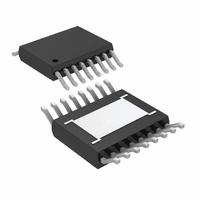
LT3755IMSE#PBF Linear Technology, LT3755IMSE#PBF Datasheet - Page 17

LT3755IMSE#PBF
Manufacturer Part Number
LT3755IMSE#PBF
Description
IC LED DRVR HP CONS CURR 16-MSOP
Manufacturer
Linear Technology
Type
High Power, Constant Currentr
Datasheet
1.LT3755EUDPBF.pdf
(26 pages)
Specifications of LT3755IMSE#PBF
Constant Current
Yes
Constant Voltage
Yes
Topology
Flyback, Low Side, PWM, SEPIC, Step-Down (Buck), Step-Up (Boost)
Number Of Outputs
1
Internal Driver
No
Type - Primary
Automotive
Type - Secondary
White LED
Frequency
100kHz ~ 1MHz
Voltage - Supply
4.5 V ~ 40 V
Voltage - Output
75V
Mounting Type
Surface Mount
Package / Case
16-MSOP Exposed Pad
Operating Temperature
-40°C ~ 125°C
Current - Output / Channel
1A
Internal Switch(s)
Yes
Lead Free Status / RoHS Status
Lead free / RoHS Compliant
Efficiency
-
Available stocks
Company
Part Number
Manufacturer
Quantity
Price
applicaTions inForMaTion
The inductor and output capacitor are chosen based on
performance, size and cost. The compensation resistor
and capacitor at VC are selected to optimize control loop
response and stability. For typical LED applications, a
2.2nF compensation capacitor at VC is adequate, and
a series resistor should always be used to increase the
slew rate on the VC pin to maintain tighter regulation of
LED current during fast transients on the input supply to
the converter.
Board Layout
The high speed operation of the LT3755 demands careful
attention to board layout and component placement. The
exposed pad of the package is the only GND terminal of
the IC and is also important for thermal management of
the IC. It is crucial to achieve a good electrical and thermal
contact between the exposed pad and the ground plane of
the board. To reduce electromagnetic interference (EMI), it
is important to minimize the area of the high dV/dt switching
node between the inductor, switch drain and anode of the
Schottky rectifier. Use a ground plane under the switching
8V TO
L1: WÜRTH ELEKTRONIK 744870220
M1: VISHAY SILICONIX SI7454DP
D1: DIODES INC. - PDS5100
M2: VISHAY SILICONIX SI2318DS
40V
V
IN
INTV
CC
100k
C1
4.7µF
50V
0.01µF
187k
1M
0.001µF
28.7k
375kHz
SHDN/UVLO
V
CTRL
OPENLED
PWM
SS
RT
V
REF
C
20W SEPIC LED Driver
30k
LT3755-2
V
GND
IN
PWMOUT
INTV
SENSE
GATE
ISP
ISN
FB
CC
C2
4.7µF
10V
25k
22µH
L1A
511k
M1
0.015
2.2µF
50V
C4
L1B
node to eliminate interplane coupling to sensitive signals.
The lengths of the high dI/dt traces: 1) from the switch
node through the switch and sense resistor to GND, and
2) from the switch node through the Schottky rectifier and
filter capacitor to GND should be minimized. The ground
points of these two switching current traces should come
to a common point then connect to the ground plane under
the LT3755. Likewise, the ground terminal of the bypass
capacitor for the INTV
the GND of the switching path. Typically this requirement
will result in the external switch being closest to the IC,
along with the INTV
the compensation network and other DC control signals
should be star connected to the underside of the IC. Do
not extensively route high impedance signals such as FB
and VC, as they may pick up switching noise. In particular,
avoid routing FB and PWMOUT in parallel for more than
a few millimeters on the board. Minimize resistance in
series with the SENSE input to avoid changes (most likely
reduction) to the switch current limit threshold.
100V
D1
5A
0.1
LT3755/LT3755-1/LT3755-2
M2
37551 TA04a
1A
20W
LED
STRING
C3
4.7µF
50V
CC
100
95
90
85
80
CC
bypass capacitor. The ground for
0
regulator should be placed near
V
I
LED
OUT
= 1A
= 18V
10
Efficiency vs V
V
IN
20
(V)
IN
30
37551 TA04b
37551fd
40


