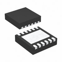
LT3498EDDB#TRPBF Linear Technology, LT3498EDDB#TRPBF Datasheet - Page 16

LT3498EDDB#TRPBF
Manufacturer Part Number
LT3498EDDB#TRPBF
Description
IC LED DRVR WT/OLED BCKLGT 12DFN
Manufacturer
Linear Technology
Type
Backlight, OLED, White LEDr
Datasheet
1.LT3498EDDBTRMPBF.pdf
(24 pages)
Specifications of LT3498EDDB#TRPBF
Topology
PWM, Step-Up (Boost)
Number Of Outputs
1
Internal Driver
Yes
Type - Primary
Backlight
Type - Secondary
OLED, White LED
Frequency
1.8MHz ~ 2.8MHz
Voltage - Supply
2.5 V ~ 12 V
Voltage - Output
32V
Mounting Type
Surface Mount
Package / Case
12-DFN
Operating Temperature
-40°C ~ 85°C
Current - Output / Channel
20mA
Internal Switch(s)
Yes
Lead Free Status / RoHS Status
Lead free / RoHS Compliant
Efficiency
-
Available stocks
Company
Part Number
Manufacturer
Quantity
Price
LT3498
Maximum Output Load Current
The maximum output current of a particular LT3498
circuit is a function of several circuit variables. The fol-
lowing method can be helpful in predicting the maximum
load current for a given circuit:
Step 1: Calculate the peak inductor current:
where I
tance value in Henrys and V
boost circuit.
Step 2: Calculate the inductor ripple current:
where V
If the inductor ripple current is less then the peak current,
then the circuit will only operate in discontinuous conduc-
tion mode. The inductor value should be increased so
that I
to operate only in discontinuous mode, but the output
current capability will be reduced.
Step 3: Calculate the average input current:
APPLICATIONS INFORMATION—OLED DRIVER
16
I
I
I
PK
RIPPLE
IN AVG
RIPPLE
(
=
LIMIT
OUT2
I
LIMIT
)
=
=
< I
(
I
is 0.3A for the OLED driver. L is the induc-
is the desired output voltage.
V
PK
PK
+
OUT
–
V
. An application circuit can be designed
IN
I
2
RIPPLE
+
•
2
400 10
1
–
L
V
•
amps
IN
L
IN
)
•
is the input voltage to the
–
150 10
9
amps
•
–
9
amps
Step 4: Calculate the nominal output current:
Step 5: Derate output current:
For low output voltages the output current capability will
be increased. When using output disconnect (load current
taken from V
drop in the PMOS switch to be higher resulting in reduced
output current capability than those predicted by the
preceding equations.
Inrush Current
When V
while the output capacitor is discharged, a higher level of
inrush current will fl ow through the inductor and integrated
Schottky diode into the output capacitor. Conditions that
increase inrush current include a larger more abrupt voltage
step at V
and an inductor with a low saturation current. While the
internal diode is designed to handle such events, the inrush
current should not be allowed to exceed 1A. For circuits
that use output capacitor values within the recommended
range and have input voltages of less than 5V, inrush cur-
rent remains low, posing no hazard to the device. In cases
where there are large steps at V
a large capacitor is used at the CAP2 pin, inrush current
should be measured to ensure safe operation.
I
I
OUT
OUT NOM
(
= I
IN
IN
is stepped from ground to the operating voltage
OUT(NOM)
, a larger output capacitor tied to the CAP2 pin,
)
OUT2
=
I
IN AVG
), these higher currents will cause the
(
• 0.7 amps
V
)
OUT
•
V
IN
2
• .
0 75
IN
(more than 5V) and/or
amps
3498fa


