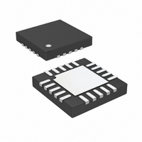
LTC3209EUF-2#TRPBF Linear Technology, LTC3209EUF-2#TRPBF Datasheet - Page 18

LTC3209EUF-2#TRPBF
Manufacturer Part Number
LTC3209EUF-2#TRPBF
Description
IC LED DRIVR QVGA DISPLAY 20-QFN
Manufacturer
Linear Technology
Type
QVGA Display (I²C Interface)r
Datasheet
1.LTC3209EUF-1PBF.pdf
(20 pages)
Specifications of LTC3209EUF-2#TRPBF
Topology
Step-Up (Boost), Switched Capacitor (Charge Pump)
Number Of Outputs
8
Internal Driver
Yes
Type - Primary
Backlight
Type - Secondary
White LED
Frequency
850kHz
Voltage - Supply
2.9 V ~ 4.5 V
Mounting Type
Surface Mount
Package / Case
20-QFN
Operating Temperature
-40°C ~ 85°C
Internal Switch(s)
Yes
Efficiency
94%
Lead Free Status / RoHS Status
Lead free / RoHS Compliant
Voltage - Output
-
Current - Output / Channel
-
Available stocks
Company
Part Number
Manufacturer
Quantity
Price
18
APPLICATIO S I FOR ATIO
LTC3209-1/LTC3209-2
Power Efficiency
To calculate the power efficiency (η) of a white LED driver
chip, the LED power should be compared to the input
power. The difference between these two numbers repre-
sents lost power whether it is in the charge pump or the
current sources. Stated mathematically, the power effi-
ciency is given by:
The efficiency of the LTC3209-1/LTC3209-2 depends upon
the mode in which it is operating. Recall that the
LTC3209-1/LTC3209-2 operates as a pass switch,
connecting V
I
available for a given input voltage and LED forward
voltage. When it is operating as a switch, the efficiency is
approximated by:
since the input current will be very close to the sum of the
LED currents.
At moderate to high output power, the quiescent current
of the LTC3209-1/LTC3209-2 is negligible and the expres-
sion above is valid.
Once dropout is detected at the LED pin, the LTC3209-1/
LTC3209-2 enables the charge pump in 1.5x mode.
LED
η =
η =
pin. This feature provides the optimum efficiency
P
P
P
P
LED
LED
IN
IN
BAT
=
(
(
V
V
to CPO, until dropout is detected at the
BAT
LED
U
•
•
I
I
LED
BAT
U
)
)
=
V
V
LED
BAT
W
(1x Mode)
U
In 1.5x boost mode, the efficiency is similar to that of a
linear regulator with an effective input voltage of 1.5 times
the actual input voltage. This is because the input current
for a 1.5x charge pump is approximately 1.5 times the load
current. In an ideal 1.5x charge pump, the power efficiency
would be given by:
(1.5x Mode)
Similarly, in 2x boost mode, the efficiency is similar to that
of a linear regulator with an effective input voltage of 2
times the actual input voltage. In an ideal 2x charge pump,
the power efficiency would be given by:
Thermal Management
For higher input voltages and maximum output current,
there can be substantial power dissipation in the
LTC3209-1/LTC3209-2. If the junction temperature in-
creases above approximately 150°C the thermal shut-
down circuitry will automatically deactivate the output
current sources and charge pump. To reduce maximum
junction temperature, a good thermal connection to the PC
board is recommended. Connecting the Exposed Pad to a
ground plane and maintaining a solid ground plane under
the device will reduce the thermal resistance of the pack-
age and PC board considerably.
η
IDEAL
(2x Mode)
η
IDEAL
=
P
=
P
LED
IN
P
P
LED
IN
=
(
=
V
BAT
(
(
V
V
BAT
(
LED
V
•
LED
( . )
•
1 5
•
( ) 2
•
I
LED
I
LED
•
•
I
I
LED
LED
)
)
)
)
=
=
(
(
1 5
2
.
V
•
V
LED
•
V
LED
BAT
V
320912fa
BAT
)
)


