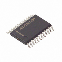
MAX6969AWG+ Maxim Integrated Products, MAX6969AWG+ Datasheet - Page 2

MAX6969AWG+
Manufacturer Part Number
MAX6969AWG+
Description
IC LED DRIVER LINEAR 24-SOIC
Manufacturer
Maxim Integrated Products
Type
Linear (Serial Interface)r
Datasheet
1.MAX6969ANG.pdf
(12 pages)
Specifications of MAX6969AWG+
Constant Current
Yes
Topology
16-Bit Shift Register, Open Drain, PWM
Number Of Outputs
16
Internal Driver
Yes
Type - Primary
General Purpose
Voltage - Supply
3 V ~ 5.5 V
Voltage - Output
5.5V
Mounting Type
Surface Mount
Package / Case
24-SOIC (7.5mm Width)
Operating Temperature
-40°C ~ 125°C
Current - Output / Channel
55mA
Internal Switch(s)
No
Low Level Output Current
37 mA
High Level Output Current
61 mA
Operating Supply Voltage
3 V to 5.5 V
Maximum Supply Current
25 mA
Maximum Power Dissipation
941 mW
Maximum Operating Temperature
+ 125 C
Mounting Style
SMD/SMT
Minimum Operating Temperature
- 40 C
Lead Free Status / RoHS Status
Lead free / RoHS Compliant
Frequency
-
Efficiency
-
Lead Free Status / Rohs Status
Lead free / RoHS Compliant
ABSOLUTE MAXIMUM RATINGS
Voltage with respect to GND.
V+ ............................................................................-0.3V to +6V
OUT_ .......................................................................-0.3V to +6V
DIN, CLK, LE, OE, SET ................................-0.3V to (V+ + 0.3V)
DOUT Current ..................................................................±10mA
OUT_ Sink Current .............................................................60mA
Total GND Current ...........................................................480mA
16-Port, 5.5V Constant-Current LED Driver
ELECTRICAL CHARACTERISTICS
(Typical Application Circuit, V+ = 3V to 5.5V, T
(Note 1)
Stresses beyond those listed under “Absolute Maximum Ratings” may cause permanent damage to the device. These are stress ratings only, and functional
operation of the device at these or any other conditions beyond those indicated in the operational sections of the specifications is not implied. Exposure to
absolute maximum rating conditions for extended periods may affect device reliability.
2
Operating Supply Voltage
Output Voltage
Standby Current
(Interface Idle, All Output Ports
High Impedance, R
Standby Current
(Interface Running, All Output
Ports High Impedance,
R
Supply Current
(Interface Idle, All Output Ports
Active Low, R
Input High Voltage
DIN, CLK, LE, OE
Input Low Voltage
DIN, CLK, LE, OE
Hysteresis Voltage
DIN, CLK, LE, OE
Input Leakage Current
DIN, CLK, LE, OE
Output High-Voltage DOUT
Output Low Voltage
Output Current OUT_
Output Leakage Current OUT_
SET
_______________________________________________________________________________________
= 360Ω)
PARAMETER
SET
= 360Ω)
SET
= 360Ω)
SYMBOL
I
I
V
IH
I
V
LEAK
V
V
∆V
OUT
V
V+
OUT
I
I
I
OH
, I
OL
+
+
+
IH
IL
I
IL
A
= T
All logic inputs at V+ or GND, DOUT
unloaded
f
or GND, DOUT unloaded
All logic inputs at V+ or GND,
DOUT unloaded
I
I
V+ = 3V to 5.5V, V
R
OE = V+, OUT_ = V+
CLK
SOURCE
SINK
SET
MIN
= 5MHz, OE = V+, DIN and LE = V+
= 360Ω
= 4mA
to T
= 4mA
MAX
, unless otherwise noted. Typical values are at V+ = 5V, T
CONDITIONS
OUT
Continuous Power Dissipation (T
Operating Temperature Range .........................-40°C to +125°C
Junction Temperature ......................................................+150°C
Storage Temperature Range .............................-65°C to +150°C
Lead Temperature (soldering, 10s) .................................+300°C
Soldering Temperature (reflow) .......................................+260°C
24-Pin TSSOP (derate 12.2mW/°C over +70°C) ..........975mW
24-Pin PDIP (derate 13.3mW/°C over +70°C)............1067mW
24 Wide SO (derate 11.8mW/°C over +70°C)..............941mW
= 0.5V to 2.5V,
- 0.5V
0.7 x
MIN
3.0
V+
V +
37
-1
A
= +70°C)
TYP
5.7
0.8
18
50
6
MAX
0.3 x
5.5
5.5
8.5
0.5
V+
+1
25
61
8
1
A
= +25°C.)
UNITS
mA
mA
mA
mA
µA
µA
V
V
V
V
V
V
V


