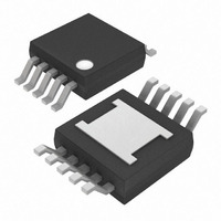
MAX7306AUB+ Maxim Integrated Products, MAX7306AUB+ Datasheet - Page 21

MAX7306AUB+
Manufacturer Part Number
MAX7306AUB+
Description
IC LED DRIVER LINEAR 10-UMAX
Manufacturer
Maxim Integrated Products
Type
Linear (I²C Interface)r
Datasheet
1.MAX7306AUB.pdf
(23 pages)
Specifications of MAX7306AUB+
Topology
PWM
Number Of Outputs
4
Internal Driver
Yes
Type - Primary
Backlight, LED Blinker
Type - Secondary
White LED
Frequency
1MHz
Voltage - Supply
1.62 V ~ 3.6 V
Mounting Type
Surface Mount
Package / Case
10-MSOP Exposed Pad, 10-HMSOP, 10-eMSOP
Operating Temperature
-40°C ~ 125°C
Current - Output / Channel
25mA
Internal Switch(s)
No
Lead Free Status / RoHS Status
Lead free / RoHS Compliant
Voltage - Output
-
Efficiency
-
Lead Free Status / Rohs Status
Details
nominally 31ms after the start of a valid serial transfer,
the interface resets itself and sets up SDA as an input.
The MAX7306/MAX7307 then waits for another START
condition.
Serial interfaces SDA, SCL (and AD0 for the MAX7306)
remain high impedance with up to 5.5V asserted on
them when the MAX7306/MAX7307 are powered down
(V
supply V
MAX7306/MAX7307’s reset threshold, all I/O ports
become high impedance. Ports P2 through P4 remain
high impedance to signals between 0V and the port
supply V
Port P1 goes high impedance to signals up to 5.5V. If a
signal outside this range is applied to a port, the port’s
protection diodes clamp the input signal to V
as appropriate. If the MAX7307’s V
input signal, the port pulls up V
diode effectively powers any load on V
signal. This behavior is safe if the current through each
protection diode is limited to 10mA.
If it is important that I/O ports remain high impedance
when all the supplies are powered down, including
the port supply V
or parasitic path for the MAX7306/MAX7307 input signals
to drive current into either the regulator providing V
or other circuits powered from V
achieve this is with a series small-signal Schottky
diode, such as the BAT54, between the port supply
and the V
The open-drain output configuration of the ports allows
them to level translate the outputs to lower (but not
higher) voltages than the V
pullup resistor converts the high-impedance, logic-high
condition to a positive voltage level. Connect the resis-
tor to any voltage up to V
inputs, a pullup resistor value of 220kΩ is a good start-
ing point. Use a lower resistance to improve noise
immunity, in applications where power consumption is
less critical, or where a faster rise time is needed for a
given capacitive load.
When driving LEDs, use a resistor in series with the
LED to limit the LED current to no more than 25mA.
Choose the resistor value according to the following
formula:
DD
SMBus/I
= 0V), independent of the voltages on the port
LA
LA
R
LA
LED
. When V
for the MAX7307 and V
input.
= (V
Applications Information
LA
______________________________________________________________________________________
SUPPLY
, then ensure that there is no direct
DD
2
= 0V, or if V
C Interfaced 4-Port, Level-Translating
- V
LA
I/O Level Translation
LED
LA
. For interfacing CMOS
Driving LED Loads
LA
LA
supply. An external
- V
DD
, and the protection
. One simple way to
LA
OL
DD
for the MAX7306.
Hot Insertion
LA
is lower than the
) / I
falls below the
from the input
LED
LA
or 0V,
LA
where:
For example, to operate a 2.2V red LED at 20mA from a
5V supply, R
The MAX7306/MAX7307 can sink current from loads
drawing more than 25mA by sharing the load across
multiple ports configured as open-drain outputs. Use at
least one output per 25mA of load current; for example,
drive a 90mA white LED with four ports.
The register structure of the MAX7306/MAX7307 allows
only one port to be manipulated at a time. Do not con-
nect ports directly in parallel because multiple ports
cannot be switched high or low at the same time, which
is necessary to share a load safely. Multiple ports can
drive high-current LEDs because each port can use its
own external current-limiting resistor to set that port’s
current through the LED.
The MAX7306/MAX7307 operate with a V
ply voltage of 1.62V to 3.6V. Bypass V
0.1µF capacitor as close as possible to the device. The
port supply V
between 1.40V and 5.5V and bypassed with a 0.1µF
capacitor as close as possible to the device. The V
supply and port supply are independent and can be
connected to different voltages or the same supply as
required.
Power supplies V
either order or together.
For the MAX7307, when a push-pull port is acting as an
input referenced to V
greater than V
GPIOs and LED Drivers
Driving Load Currents Higher than 25mA
R
the LED (Ω)
V
LED (V)
V
V
MAX7307 when sinking I
I
LED
SUPPLY
LED
OL
LED
is the desired operating current of the LED (A).
is the output low voltage of the MAX7306/
is the forward voltage of the LED (V)
is the resistance of the resistor in series with
LED
CC
is the supply voltage used to drive the
LA
= (5 - 2.2 - 0.2) / 0.020 = 100Ω.
- 0.3V.
Power-Supply Considerations
is connected to a supply voltage
DD
CC
and V
, make sure the VLA voltage is
LA
LED
can be sequenced in
(V)
DD
DD
to GND with a
power-sup-
DD
21


