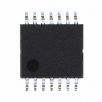
LX1744CPW Microsemi Analog Mixed Signal Group, LX1744CPW Datasheet - Page 7

LX1744CPW
Manufacturer Part Number
LX1744CPW
Description
IC LED DRVR WT/CLR BCKLT 14TSSOP
Manufacturer
Microsemi Analog Mixed Signal Group
Type
Backlight, White LED, Color LEDr
Datasheet
1.LX1744CPW.pdf
(16 pages)
Specifications of LX1744CPW
Constant Current
Yes
Topology
PWM, Step-Up (Boost)
Number Of Outputs
2
Internal Driver
Both
Type - Primary
Backlight
Type - Secondary
Color, White LED
Voltage - Supply
1.6 V ~ 6 V
Voltage - Output
25V
Mounting Type
Surface Mount
Package / Case
14-TSSOP
Operating Temperature
-40°C ~ 85°C
Current - Output / Channel
100mA
Internal Switch(s)
Yes
Efficiency
90%
Lead Free Status / RoHS Status
Lead free / RoHS Compliant
Frequency
-
Available stocks
Company
Part Number
Manufacturer
Quantity
Price
Company:
Part Number:
LX1744CPW
Manufacturer:
Microsemi Analog Mixed Signal
Quantity:
135
Copyright © 2000
Rev. 1.1b, 2005-03-01
F
(PFM) boost converter that is optimized for large step-up
voltage applications like LCD biasing and LED drive.
switch “off time” of 300ns, converter switching is enabled
when the feedback voltage (V
reference voltage or the ADJ pin voltage managed by the
reference logic block (see Block Diagram).
occurs, the feedback comparator activates the switching
logic, pulling the gate of the power MOSFET high. This in
turn connects the boost inductor to ground causing current
to flow building up the energy stored in the inductor. The
output remains “on”, until the inductor current ramps up to
the peak current level set either by the CS pin programming
resistor (R
reference threshold for the LCD bias output. During this
switch cycle, the load is powered from energy stored in the
output capacitor. Once the peak inductor current value is
achieved, the driver output is turned off, for the fixed off-
time period of 300ns, allowing a portion of the energy
stored in the inductor to be delivered to the load causing
output voltage to rise at the input to the feedback circuit. If
the voltage at the feedback pin is less than the internal
reference at the end of the off-time period, the output
switches the power MOSFET “on” and the inductor
charging cycle repeats until the feedback pin voltage is
greater than the internal reference.
switching behavior is shown in Figure 12.
LCD B
voltage divider (Figure 3), connected to the feedback pin,
programs the output voltage.
UNCTIONAL
V
The LX1744 is a dual output Pulse Frequency Modulated
Operating in a pseudo-hysteretic mode with a fixed
Selecting the appropriate values for LCD Bias output
OUT
V
IAS
BAT
I N T E G R A T E D
CS
– O
= 1.6V to 6.0V
) in the case of the LED driver or by an internal
Figure 3 – LCD Bias Output Voltage
D
UTPUT
ESCRIPTION
11861 Western Avenue, Garden Grove, CA. 92841, 714-898-8121, Fax: 714-893-2570
R
R
V
1
2
OLTAGE
FB
P
) falls below the bandgap
P R O D U C T S
ROGRAMMING
Typical converter
SW
A P P L I C A T I O N N O T E
LX1744
Integrated Products Division
When this
FB
Microsemi
Dual Output Boost – LED Driver / LCD Bias
Using a value between 40kΩ and 75kΩ for R
in most applications.
following equation (where V
LCD B
of the voltage output via an adjustment pin (ADJ). Any
voltage applied to the adjustment pin works in conjunction
with the internal reference logic.
automatically utilize the internal reference when no signal
is detected or when the adjustment signal voltage is below
approximately 0.6V.
to ground (Figure 4) that works with an external resistor to
create a low-pass filter. This allows a direct PWM (f
100KHz) signal input to be used for the voltage adjustment
signal. (Consequently a DC bias signal can also be used).
selecting a value for R
is equal to the reference voltage (eq. 2)
approximately 1% or 40dB down from the nominal
reference. When using a PWM with a frequency that is
The LX1744 allows for the dynamic adjustment of the
This adjustment pin includes an internal 50pF capacitor
Different PWM signal levels can be accommodated by
Ideally the resultant ripple on the ADJ pin should be
IAS
V
Figure 5 – LCD Bias Adjustment Input Filter
ADJ
LX1744
– O
Reference
Figure 4 – LCD Bias Adjustment Input
P
=
Logic
RODUCTION
V
UTPUT
LX1744
PWM
R =
⋅
Duty
1
50pF
ADJ
V
PWM
OLTAGE
R
Cycle
2.5MΩ
R
2
such that the filtered V
V
1
D
REF
OUT
ADJ
C
ATASHEET
can be determined by the
ADJ
V
⋅
REF
= 1.19V nominal):
-
⎛
⎜
⎜
⎝
A
V
2
DJUSTMENT
REF
5 .
R
M
R
R
ADJ_2
ADJ_1
2
ADJ_1
Ω
5 .
The LX1744 will
+
M
R
Ω
PWM
2
_
works well
1
⎞
⎟
⎟
⎠
LX1744
ADJ
PWM
value
eq. 1
eq. 2
≥
Page 7


