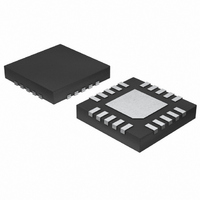
MAX8790ETP+ Maxim Integrated Products, MAX8790ETP+ Datasheet - Page 2

MAX8790ETP+
Manufacturer Part Number
MAX8790ETP+
Description
IC LED DRVR WHITE BCKLGT 20-TQFN
Manufacturer
Maxim Integrated Products
Type
Backlight, White LEDr
Datasheet
1.MAX8790ETP.pdf
(24 pages)
Specifications of MAX8790ETP+
Topology
PWM, Step-Up (Boost)
Number Of Outputs
6
Internal Driver
No
Type - Primary
Backlight
Type - Secondary
White LED
Frequency
1MHz
Voltage - Supply
4.5 V ~ 5.5 V, 5.5 V ~ 26 V
Voltage - Output
5V
Mounting Type
Surface Mount
Package / Case
20-TQFN Exposed Pad
Operating Temperature
-40°C ~ 85°C
Current - Output / Channel
25mA
Internal Switch(s)
Yes
Low Level Output Current
1000000 uA (Typ)
High Level Output Current
25.75 mA
Operating Supply Voltage
4.5 V to 26 V
Maximum Supply Current
2 mA
Maximum Power Dissipation
1349 mW
Maximum Operating Temperature
+ 85 C
Mounting Style
SMD/SMT
Minimum Operating Temperature
- 40 C
Lead Free Status / RoHS Status
Lead free / RoHS Compliant
Efficiency
-
Lead Free Status / Rohs Status
Lead free / RoHS Compliant
ABSOLUTE MAXIMUM RATINGS
IN, SHDN, to GND .................................................-0.3V to +28V
FB_ to GND ............................................................-0.3V to +28V
V
ISET, CCV, CS, FSET, CPLL, EXT to GND .-0.3V to (V
Continuous Power Dissipation (T
Six-String White LED Driver with Active
Current Balancing for LCD Panel Applications
Stresses beyond those listed under “Absolute Maximum Ratings” may cause permanent damage to the device. These are stress ratings only, and functional
operation of the device at these or any other conditions beyond those indicated in the operational sections of the specifications is not implied. Exposure to
absolute maximum rating conditions for extended periods may affect device reliability.
ELECTRICAL CHARACTERISTICS
(Circuit of Figure 1. V
2
IN Input Voltage Range
IN Quiescent Current
V
V
V
STEP-UP CONVERTER
EXT High Level
EXT Low Level
EXT On-Resistance
EXT Sink/Source Current
OSC High-Level Threshold
OSC Midlevel Threshold
OSC Low-Level Threshold
Operating Frequency
Minimum Duty Cycle
Maximum Duty Cycle
CS Trip Voltage
CONTROL INPUT
SHDN Logic-Input High Level
SHDN Logic-Input Low Level
BRT, ENA Logic-Input High Level
BRT, ENA Logic-Input Low Level
CC
20-Pin Thin QFN (derate 16.9mW/°C above +70°C) ...1349mW
CC
CC
CC
, BRT, ENA, OSC, OV to GND ...........................-0.3V to +6V
_______________________________________________________________________________________
Output voltage
Short-Circuit Current
UVLO Threshold
PARAMETER
IN
= 12V, V
SHDN
A
= +70°C)
= V
V
V
V
SHDN = GND
V
Rising edge, hysteresis = 20mV
10mA from EXT to GND
-10mA from EXT to V
EXT high or low
EXT forced to 2V
V
V
V
PWM mode
Pulse skipping, no load
Duty cycle = 75%
IN
CC
SHDN
SHDN
OSC
OSC
OSC
IN
= V
= bypassed to GND through 1µF cap
, CCV = 0.1µF, T
= V
= open
= GND
CC
= high
= 5V, 6V < V
CC
CC
+ 0.3V)
IN
CC
A
CONDITIONS
< 26V, 0 < I
= 0°C to +85°C, unless otherwise noted. Typical values are at T
V
V
IN
IN
Operating Temperature Range ...........................-40°C to +85°C
Junction Temperature ......................................................+150°C
Storage Temperature Range .............................-60°C to +150°C
Lead Temperature (soldering, 10s) .................................+300°C
= 26V
= V
VCC
CC
< 10mA
= 5V
V
V
4.00
MIN
675
450
4.5
5.5
4.7
0.1
0.4
1.5
0.9
2.1
2.1
CC
CC
15
94
85
-
-
TYP
4.25
V
750
500
100
5.0
1.0
56
10
95
CC
1
1
0
2
1
0
V
MAX
26.0
4.45
130
825
550
115
5.5
5.3
0.1
2.0
0.4
1.1
0.8
0.8
CC
10
2
2
5
-
A
= +25°C.)
UNITS
MHz
kHz
mA
mA
mV
µA
Ω
%
%
V
V
V
V
V
A
V
V
V
V
V
V
V


