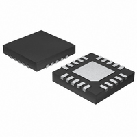
MAX16834ATP+ Maxim Integrated Products, MAX16834ATP+ Datasheet - Page 21

MAX16834ATP+
Manufacturer Part Number
MAX16834ATP+
Description
IC LED DRIVR HIGH BRIGHT 20-TQFN
Manufacturer
Maxim Integrated Products
Type
HBLED Driverr
Datasheet
1.MAX16834ATP.pdf
(23 pages)
Specifications of MAX16834ATP+
Topology
PWM, SEPIC, Step-Down (Buck), Step-Up (Boost)
Number Of Outputs
1
Internal Driver
No
Type - Primary
Automotive, Backlight
Type - Secondary
High Brightness LED (HBLED), RGB
Frequency
100kHz ~ 1MHz
Voltage - Supply
4.75 V ~ 28 V
Mounting Type
Surface Mount
Package / Case
20-TQFN Exposed Pad
Operating Temperature
-40°C ~ 125°C
Internal Switch(s)
Yes
Operating Supply Voltage
4.75 V to 28 V
Maximum Supply Current
10 mA
Maximum Power Dissipation
2051 mW
Maximum Operating Temperature
+ 125 C
Mounting Style
SMD/SMT
Minimum Operating Temperature
- 40 C
Lead Free Status / RoHS Status
Lead free / RoHS Compliant
Voltage - Output
-
Current - Output / Channel
-
Efficiency
-
Lead Free Status / Rohs Status
Lead free / RoHS Compliant
Typically, there are two sources of noise emission in a
switching power supply: high di/dt loops and high dv/dt
surfaces. For example, traces that carry the drain cur-
rent often form high di/dt loops. Similarly, the heatsink
of the MOSFET connected to the device drain presents
a dv/dt source; therefore, minimize the surface area of
the heatsink as much as is compatible with the MOS-
FET power dissipation or shield it. Keep all PCB traces
carrying switching currents as short as possible to mini-
mize current loops. Use ground planes for best results.
Careful PCB layout is critical to achieve low switching
losses and clean, stable operation. Use a multilayer
board whenever possible for better noise immunity and
power dissipation. Follow these guidelines for good
PCB layout:
1) Use a large contiguous copper plane under the
2) Isolate the power components and high-current
3) Keep the high-current paths short, especially at the
High-Power LED Driver with Integrated High-Side LED
Current Sense and PWM Dimming MOSFET Driver
MAX16834 package. Ensure that all heat-dissipat-
ing components have adequate cooling.
path from the sensitive analog circuitry.
ground terminals. This practice is essential for sta-
ble, jitter-free operation. Keep switching loops short
such that:
a) The anode of D1 must be connected very close
to the drain of the MOSFET Q1.
______________________________________________________________________________________
Layout Recommendations
4) Connect PGND and SGND to a star-point configura-
5) Keep the power traces and load connections short.
6) Route high-speed switching nodes away from the
7) To prevent discharge of the compensation capaci-
b) The cathode of D1 must be connected very
c) C
tion.
This practice is essential for high efficiency. Use
thick copper PCBs (2oz vs.1oz) to enhance full-load
efficiency.
sensitive analog areas. Use an internal PCB layer
for the PGND and SGND plane as an EMI shield to
keep radiated noise away from the device, feed-
back dividers, and analog bypass capacitors.
tors during the off-time of the dimming cycle,
ensure that the PCB area close to these compo-
nents has extremely low leakage. Discharge of
these capacitors due to leakage results in reduced
performance of the dimming circuitry.
close to C
connected directly to the ground plane.
OUT
and the current-sense resistor R8 must be
OUT
.
21


