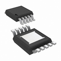
LM3409HVMY/NOPB National Semiconductor, LM3409HVMY/NOPB Datasheet - Page 14

LM3409HVMY/NOPB
Manufacturer Part Number
LM3409HVMY/NOPB
Description
IC LED DRIVR HIGH BRIGHT 10-MSOP
Manufacturer
National Semiconductor
Series
PowerWise®r
Type
HBLED Driverr
Datasheet
1.LM3409MYNOPB.pdf
(30 pages)
Specifications of LM3409HVMY/NOPB
Constant Current
Yes
Topology
PWM, Step-Down (Buck)
Number Of Outputs
1
Internal Driver
No
Type - Primary
Automotive
Type - Secondary
High Brightness LED (HBLED)
Voltage - Supply
6 V ~ 75 V
Mounting Type
Surface Mount
Package / Case
10-MSOP Exposed Pad, 10-HMSOP, 10-eMSOP
Operating Temperature
-40°C ~ 125°C
Internal Switch(s)
Yes
Efficiency
97%
Lead Free Status / RoHS Status
Lead free / RoHS Compliant
Voltage - Output
-
Frequency
-
Current - Output / Channel
-
Other names
LM3409HVMYTR
Available stocks
Company
Part Number
Manufacturer
Quantity
Price
Company:
Part Number:
LM3409HVMY/NOPB
Manufacturer:
VISHAY
Quantity:
15 600
www.national.com
INPUT CAPACITORS
Input capacitors are selected using requirements for mini-
mum capacitance and RMS ripple current. The PFET current
during t
discharge the difference between I
current (I
charges up the input capacitors with I
capacitance (C
voltage ripple (Δv
equal to the change in voltage across C
supplies the load current. A good starting point for selection
of C
selected as follows:
An input capacitance at least 75% greater than the calculated
C
current rating (I
used:
Since this approximation assumes there is no inductor ripple
current, the value should be increased by 10-30% depending
on the amount of ripple that is expected. Ceramic capacitors
are the best choice for input capacitors for the same reasons
mentioned in the Buck Converters with Output Capacitors
section. Careful selection of the capacitor requires checking
capacitance ratings at the nominal operating voltage and tem-
perature.
P-CHANNEL MosFET (PFET)
The LM3409/09HV requires an external PFET (Q1) as the
main power MosFET for the switching regulator. Q1 should
have a voltage rating at least 15% higher than the maximum
input voltage to ensure safe operation during the ringing of
the switch node. In practice all switching converters have
some ringing at the switch node due to the diode parasitic
capacitance and the lead inductance. The PFET should also
have a current rating at least 10% higher than the average
transistor current (I
The power rating is verified by calculating the power loss
(P
on-resistance (R
IN-MIN
T
) using the RMS transistor current (I
IN
is to use Δv
ON
value is recommended. To determine the RMS input
IN
is approximately I
) during t
IN-MIN
IN-RMS
DS-ON
IN-MAX
IN-MAX
T
ON
):
) is selected using the maximum input
):
) the following approximation can be
. During t
) which can be tolerated. Δv
of 2% to 10% of V
LED
, therefore the input capacitors
OFF
LED
, the input voltage source
IN
and the average input
. The minimum input
T-RMS
IN
during t
IN
. C
) and the PFET
IN-MIN
ON
IN-MAX
when it
can be
is
14
It is important to consider the gate charge of Q1. As the input
voltage increases from a nominal voltage to its maximum in-
put voltage, the COFT architecture will naturally increase the
switching frequency. The dominant switching losses are de-
termined by input voltage, switching frequency, and PFET
total gate charge (Q
remove charge Q
to turn it on and off. This occurs more often at higher switching
frequencies which requires more current from the internal
regulator, thereby increasing internal power dissipation and
eventually causing the LM3409/09HV to thermally cycle. For
a given range of operating points the only effective way to
reduce these switching losses is to minimize Q
A good rule of thumb is to limit Q
frequency remains below 300kHz for the entire operating
range then a larger Q
small R
be no choice but to use a PFET with Q
When using a PFET with Q
(C
that peak current detection through R
the charging of the PFET input capacitance during switching,
which can cause false triggering of the peak detection com-
parator. Instead, C
to the CSN pin which will cause a small DC offset in V
ultimately I
gering.
In general, the PFET should be chosen to meet the Q
ification whenever possible, while minimizing R
minimize power losses while ensuring the part functions cor-
rectly over the full operating range.
RE-CIRCULATING DIODE
A re-circulating diode (D1) is required to carry the inductor
current during t
Schottky diode due to low forward voltage drop and near-zero
reverse recovery time. Similar to Q1, D1 must have a voltage
rating at least 15% higher than the maximum input voltage to
ensure safe operation during the ringing of the switch node
and a current rating at least 10% higher than the average
diode current (I
The power rating is verified by calculating the power loss
through the diode. This is accomplished by checking the typ-
ical diode forward voltage (V
product datasheet and calculating as follows:
In general, higher current diodes have a lower V
in better performing packages minimizing both power losses
and temperature rise.
F
) should not be connected to the VIN pin. This will ensure
DS-ON
LED
and a high voltage rating is required, there may
, however it avoids the problematic false trig-
D
OFF
):
g
F
from the input capacitance of Q1 in order
. The most efficient choice for D1 is a
g
). The LM3409/09HV has to provide and
should be connected from the VCC pin
g
can be considered). If a PFET with
g
> 30nC, the bypass capacitor
D
) from the I-V curve on the
g
< 30nC (if the switching
SNS
g
> 30nC.
is not affected by
DS-ON
g
.
D
and come
. This will
CST
g
spec-
and


